


Abstract
Here in in this article an attempt has been made to study various types of microscopes in detail. In this review paper we have discussed various types of microscopes which are classified as electron microscopes, x-ray microscope and probe microscopes. Also, the various subtypes of each of these microscopes have been presented in this paper. This paper focuses on the historical developments, Principles of operation, instrumentation, advantages and limitations of the various types and subtypes of the microscopes. The properties of the materials at nanoscale depend upon their size, shape and nature. As nanomaterials are invisible, we require various advanced characterization techniques to reveal their morphology. The various advanced characterization techniques required for the analysis of nanomaterials are thoroughly discussed in this paper.
Keywords: Electron microscope; Probe microscope; X-Ray microscope; Fluorescence microscope
Electron Microscope
This type of microscope uses beams of accelerated electrons as a source of illumination. The wavelength of an electron is 100,000 times shorter than the visible photons. Consequently, electron microscopes are having higher resolving power than optical microscopes. The electron microscope can be further sub classified into different types such as SEM and TEM based upon their construction and type of action and information we get. Another advanced type of electron microscope is Combined SEM and TEM where two types of electron microscopes are combined together.
Scanning Electron Microscope:
Scientists and engineers have been striving to achieve high magnification and resolution of microscopic and nanoscale entities. Numerous researchers have made efforts in this field, with a notable and successful contribution by German physicist Ernest Ruska and German electrical engineer Max Knoll in 1931. The scanning electron microscope (SEM) is a type of electron microscope that creates images by scanning a surface with a focused beam of electrons. These electrons interact with the atoms in the sample, generating various signals that provide information about the sample’s surface topography and composition. The electron beam scans in a raster pattern, and the beam’s position is combined with the intensity of the detected signal to form an image. SEM is used to observe specimen surfaces, where a fine electron beam causes the emission of secondary electrons from the surface. The surface topography can be observed in two dimensions. When the specimen is struck by an incident electron beam, it emits X-rays and three types of electrons: primary backscattered electrons, secondary electrons, and Auger electrons. SEM devices primarily utilize primary backscattered electrons [1-7].
Instrumentation and Working of SEM:
The essential components of an SEM include the electron
source (gun), electron lenses, sample stage, detectors for all
relevant signals, display/data output device, power supply,
vacuum system, cooling system, infrastructure requirements,
vibration-free flooring, and a room free from ambient magnetic
and electric fields.
a) Electron Gun: An electron gun generates electron
beams, which can be emitted either by heating a filament
(thermionic emission) or by applying a high potential difference
(field emission). Electron microscopes typically use magnetic
lenses. To create a strong magnetic lens, the density of magnetic
lines must be increased, achieved through a precisely fabricated
pole piece with a narrow gap. A key characteristic of a magnetic
lens is that changing the current passing through the coil alters the
lens’s strength, a feature not possible with optical microscopes.
b) Condenser lens and objective lens: When a lens is
positioned below the electron gun, it allows for the adjustment
of the electron beam diameter. SEM requires a finely focused
electron beam (probe), achieved by using a two-stage lens system
that combines the condenser and objective lenses. Consequently,
the electron beam from the electron gun is focused by these two
lenses, producing a small electron probe.
c) Specimen stage: In an electron microscope, specimens
are observed at high magnification and resolution. The SEM
specimen stage is designed to allow various movements, including:
(a) horizontal movement, (b) vertical movement, (c) specimen
tilting, and (d) rotation. The X and Y movements are used to select
the field of view, while the Z movement adjusts image resolution
and depth of focus.
d) Secondary Electron Detector: When a specimen in an
electron microscope is bombarded by electrons from an electron
gun, it emits secondary electrons. A secondary electron detector,
with a scintillator coated on its tip and a high potential difference
applied, detects these secondary electrons. The emitted electrons
are attracted to the high voltage, generating light. When the
electron beam strikes the sample, some incident electrons interact
with the nucleus of atoms. These negatively charged electrons are
attracted to the positively charged nucleus, encircle it, and then
exit the sample without losing speed, becoming backscattered
electrons. Secondary electrons originate from surface regions,
while backscattered electrons re-emerge from the sample.
Backscattered and secondary electrons provide different types
of information. Backscattered electrons are highly sensitive to
atomic numbers, with brighter regions indicating atoms with
higher atomic numbers and darker regions indicating atoms
with lower atomic numbers. Secondary electrons offer surface
information about the sample.
e) Secondary Electrons: Secondary electrons originate
from the surface of the sample being studied, generated through
inelastic interactions between the primary electron beam and the
sample. These electrons have lower energy compared to primary
or backscattered electrons and are essential for determining the
topography of the sample (Figure 1).
Principle of SEM
A monochromatic beam directed at a solid substrate surface generates various signals, contingent on the substrate’s composition and structure. In SEM imaging, backscattered or secondary electrons are commonly employed, with their intensity linked to the atomic number of the materials involved. Each backscattered electron can be captured, amplified, and utilized to modulate the brightness spot on a cathode ray tube (CRT). To acquire signals from an area, the electron beam scans over the specimen surface via two pairs of electromagnetic deflection coils, synchronized with the CRT beam. The signals are transferred point by point, generating a signal map of the scanned region displayed on a long-persistence phosphor CRT screen. Changes in brightness indicate variations in specific properties within the scanned area of the specimen (Figure 2).
The scattering cross section for back-scattered electrons is given as [2], where, Z is atomic number and E is electric field.
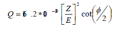


Here the cross-section is proportional to Z2. Hence, the backscattered electrons are used for the Z contrast or for compositional mapping.
Limitation of SEM:
a) Sample Preparation Requirements: SEM requires
samples to be conductive or coated with a conductive material
(e.g., gold, carbon) to prevent charging effects caused by the
electron beam. Sample preparation can be time-consuming and
may alter the sample’s natural properties.
b) Vacuum Environment: SEM operates under high
vacuum conditions, which can limit the analysis of certain samples,
especially those that are volatile, hydrated, or sensitive to vacuum
conditions. Some samples may require specialized sample holders
or environmental SEMs to maintain their integrity.
c) Limited Depth of Field: SEM has a shallow depth of
field, meaning that only the surface of the sample is in focus at any
given time. This can make it challenging to obtain clear images
of three-dimensional structures or samples with rough surfaces.
d) Resolution: While SEM offers high-resolution imaging
capabilities, the resolution is ultimately limited by factors such as
the electron beam energy, specimen characteristics, and detector
efficiency. Achieving sub-nanometer resolution often requires
sophisticated instrumentation and careful optimization.
e) Sample Damage: The high-energy electron beam used
in SEM can potentially damage the sample through processes
such as electron beam-induced deposition, sample heating, or
radiation damage. Minimizing beam exposure and optimizing
imaging conditions can help mitigate sample damage.
f) Limited Chemical Information: SEM provides
primarily morphological and topographical information about
samples. While energy-dispersive X-ray spectroscopy (EDS)
can be used for elemental analysis, it has limitations in terms
of sensitivity, spatial resolution, and quantification accuracy
compared to other analytical techniques like X-ray diffraction
(XRD) or X-ray photoelectron spectroscopy (XPS).
Transmission Electron Microscope
Transmission Electron Microscope is a type of electron microscope that has three essential components viz. electron gun, image producing system, imaging recording system [8-15].
Instrumentation of TEM
a) Electron gun:
An electron gun is an essential component
that generates a precisely controlled electron beam in a TEM
(Transmission Electron Microscope). Positioned at the top of
the TEM, the electron gun emits electrons that travel through
the microscope›s vacuum tube. The key elements of an electron
gun include the electron emitter, the biasing cylinder (Wehnelt
cylinder), and the anode. The electron emitter is typically a
tungsten filament covered by a control grid (Wehnelt cylinder),
which has a central aperture aligned with the vacuum tube. The
cathode, located either above or below this aperture, and the
grid are negatively charged. The anode, typically disc-shaped
with an axial hole, is positioned to receive the emitted electrons.
As electrons are emitted from the cathode, they pass through
the central aperture of the Wehnelt cylinder and are accelerated
towards the anode at high voltage, maintaining a constant energy
level. This configuration effectively focuses the electron beam to
interact with the specimen and produce a well-defined image.
b) Image Producing System:
The imaging system of an
electron microscope includes an objective lens, a movable stage
for holding the specimen, and intermediate and projector lenses.
These components collaborate to focus electrons passing through
the specimen, resulting in a significantly magnified image. The
objective lens, typically with a short focal length of approximately
1-5 mm, first forms an intermediate image from the condenser.
This intermediate image is then transmitted to the projector
lenses for further magnification. There are two types of projector
lenses: the intermediate lens, which enables greater image
magnification, and the projector lens, which generally offers even
higher magnification than the intermediate lens.
c) Image Recording System:
The image recording system
includes a fluorescent screen used for viewing and focusing on the
image, along with digital cameras capable of effectively recording
and capturing it. To maintain optimal imaging conditions, a
vacuum system prevents electron collisions with air molecules
that could disrupt their movement and focusing ability. This
vacuum system comprises a pump, gauge, valves, and power
supply, ensuring electrons move directly to form the image
without interference. The resulting image is monochromatic,
typically appearing greyish or black, designed to be easily visible
to the human eye by passing through the fluorescent screen fixed
at the base of the microscope.
Working Principle:
Transmission electron microscopy (TEM) is a microscopic technique where an electron beam passes through an ultrathin specimen, interacting with it as it traverses. Its operational principle shares similarities with light microscopy, but differs fundamentally in the use of electrons instead of light rays to focus on and produce images of the specimen. Electrons have shorter wavelengths compared to light, enabling higher resolution capabilities in TEM. Unlike light microscopes where resolution increases with shorter wavelengths, TEM achieves resolution by increasing the energy of transmitted electrons.
In TEM analysis, a thin specimen is exposed to electrons to ensure uniform electron intensity across the illuminated area. As these electrons traverse the specimen, they either undergo scattering processes or pass through unaffected, leading to a nonuniform distribution of electrons emerging from the specimen’s surface. This distribution contains detailed structural and chemical information about the specimen.
An electron microscope is designed to visualize this electron distribution in two main ways: the angular distribution of scattering, seen as diffraction patterns, and the spatial distribution of scattering, observed as contrast in specimen images. This setup enables direct observation of the specimen area that generates the diffraction pattern. The fundamental components of a transmission electron microscope are depicted in Figure 3.
Working principle of TEM:
a) The electron gun serves as a crucial source, generating a
stream of monochromatic electrons.
b) TEM operates using accelerated electron beams instead
of light, focusing them to create images.
c) The magnification capability exceeds that of a light
microscope by over 2 million times.
d) Condenser lenses 1 and 2 concentrate the stream into
a small, coherent beam. The first lens, adjustable via a spot size
knob, primarily determines the beam’s size, while the second lens,
controlled by an intensity or brightness knob, further adjusts the
spot size on the sample.
e) The condenser aperture limits the electron beam,
filtering out high-angle electrons.
f) The electron beam impacts the specimen, with a portion
of it passing through.
g) The transmitted portion is then focused by the objective
lens.
h) Optical objective and selected area metal apertures
further control the beam. The objective aperture enhances
contrast by blocking high-angle diffracted electrons, while the
selected area aperture enables examination of electron diffraction
patterns caused by the ordered arrangement of atoms in the
sample.
i) A photographic image is captured from the electrons
that have passed through the thin specimen under study. These
images strike a phosphorus image screen, generating light that
allows observation. Darker areas in the image indicate regions
where fewer electrons transmitted through the sample.

Limitation of TEM:
a) Sample Preparation: TEM requires samples to be
extremely thin (typically less than 100 nanometers) to allow
electrons to pass through. Preparing such thin samples can be
challenging and often involves techniques like ultramicrotomy
or ion milling, which can introduce artifacts. Potentially damage
sample or alter the sample’s structure.
b) Vacuum Environment: TEM operates under high
vacuum conditions, which can limit the analysis of certain samples,
especially those that are volatile or hydrated. Some samples may
require specialized sample holders or environmental TEMs to
maintain their integrity under vacuum.
c) Electron Beam Resolution: While TEM offers extremely
high resolution, the achievable resolution is ultimately limited by
factors such as the electron beam energy, specimen thickness,
and instrumental aberrations. Achieving atomic resolution often
requires sophisticated instrumentation and careful optimization.
d) Beam-sensitive Samples: Some samples are highly
sensitive to the electron beam and may undergo structural
changes or damage even at relatively low beam energies. Biological
specimens, organic materials, and certain nanomaterials are
particularly prone to beam damage.
e) Depth of Field: Similar to SEM, TEM has a limited depth
of field, meaning that only a thin section of the sample is in focus at
any given time. This can make it challenging to obtain clear images
of three-dimensional structures or samples with significant depth
variations (Table 1).

Combing SEM and TEM Together:
This instrument is called scanning transmission electron microscopy. This instrument can be applied to a TEM tool. Most modern TEM can be switched to STEM mode. In STEM mode, the beam is finally focused and scans the sample area while the image is generated by the transmitted electron. Combining Scanning Electron Microscopy (SEM) and Transmission Electron Microscopy (TEM) into a single instrument, often referred to as a “dual-beam” or “dual-mode” microscope, offers several advantages for comprehensive material characterization. Although such instruments are not commonplace, they offer significant benefits in terms of sample preparation, imaging, and analysis [16-21].
Instrument Configuration:
The instrument would likely consist of a platform that
integrates both SEM and TEM capabilities. The SEM component
would typically be used for initial sample inspection, navigation,
and coarse imaging due to its relatively large depth of field
and ease of use. The TEM component would allow for higherresolution
imaging and detailed analysis of thin sections of the
sample.
a) Sample Preparation: The combined instrument
would streamline sample preparation, as the same sample
could be examined using both SEM and TEM without the need
for additional sample handling. Initial sample inspection and
rough characterization could be performed using SEM, guiding
subsequent TEM analysis of specific regions of interest.
b) Imaging and Analysis: SEM imaging would provide
detailed surface morphology and topography information at
relatively low magnifications. TEM imaging would offer higherresolution
imaging of internal structures and thin sections of the
sample, providing atomic-scale details of crystal structure, defects,
and interfaces. Combined SEM and TEM analysis would allow for
comprehensive material characterization, including investigation
of microstructure, phase identification, chemical composition,
and elemental mapping.
Applications:
a) Material Science: Such instruments would be
invaluable for characterizing nanomaterials, nanoparticles, and
nanostructures, providing insights into their morphology, size
distribution, and crystalline structure. Biological Sciences: In
biology and life sciences, combined SEM/TEM capabilities could
facilitate the study of biological specimens, such as cells, tissues,
and biomaterials, offering detailed imaging of ultrastructure and
subcellular organelles.
b) Research and Development: Combined SEM/TEM
instruments would be essential tools for research laboratories
and industrial R&D facilities.
Limitations of combined SEM and TEM:
a) Instrument Complexity: Integrated SEM-TEM systems
are complex and require sophisticated engineering to combine
two distinct imaging modalities into a single instrument. This
complexity can lead to maintenance challenges, and longer
training times for operators.
b) Sample Preparation Challenges: Samples for combined
SEM and TEM analysis often require extensive preparation
to meet the requirements of both techniques. Achieving the
necessary thinness for TEM while maintaining conductivity or
surface topography for SEM can be challenging and may introduce
artifacts or limitations.
c) Limited Field of View: While SEM provides a wide field
of view, TEM offers higher resolution but a much narrower field of
view. Combined systems typically sacrifice some of the SEM’s field
of view to accommodate the TEM column, leading to limitations in
imaging large areas at high resolution.
d) Sequential Imaging: In most combined SEM-TEM
systems, imaging modes are sequential rather than simultaneous.
This means that switching between SEM and TEM imaging
requires physical adjustments of the sample and optics, leading to
longer analysis times and potential disruptions to sample stability.
e) Complexity of Data Interpretation: Combined SEMTEM
datasets can be complex to interpret, as they provide
complementary information from two different imaging
modalities. Integrating and correlating data from SEM and TEM
images may require advanced software tools and expertise,
especially for quantitative analysis or multi-modal imaging.
f) Limited TEM Performance: In some integrated systems,
the TEM functionality may be limited compared to standalone
TEM instruments. This can include constraints on achievable
resolution, imaging modes, or analytical capabilities, depending
on the design and specifications of the combined system.
X-Ray Microscope:
An X-ray microscope is an imaging instrument that uses X-rays instead of visible light to create high-resolution images of objects, typically on the nanometer scale [22-27].
Instrumentation of X-Ray Microscopy
a) X-ray Source: X-ray microscopes require a source of
X-ray radiation to illuminate the sample. Common X-ray sources
include X –ray tubes and Synchrotron radiations:
b) X-ray tubes: Produce X-rays by accelerating electrons to
high velocities and colliding them with a metal target.
c) Synchrotron radiation: Highly intense and tunable
X-rays are generated by accelerating charged particles (electrons
or protons) to nearly the speed of light in a synchrotron facility.
d) X-ray Optics: X-ray optics are used to focus and
manipulate the X-ray beam before it interacts with the sample.
Unlike optical microscopes, X-ray microscopes cannot use
conventional lenses due to the high energy and short wavelengths
of X-rays. Instead, X-ray optics contains Fresnel zone plate,
Multilayer mirrors, capillary optics.
e) Sample Stage: The sample stage holds the specimen and
allows for precise positioning and manipulation during imaging.
It may include mechanisms for translation, rotation, and tilt to
adjust the orientation of the sample relative to the X-ray beam.
f) Detector: X-ray detectors capture the X-rays transmitted
through or scattered by the sample to create an image.
g) X-ray CCD (charge-coupled device) cameras: Capture
X-ray photons and convert them into electronic signals for image
formation.
h) X-ray sensitive films: Traditional photographic films
that react to X-ray exposure. X-ray-sensitive scintillators coupled
with photodetectors: Convert X-ray photons into visible light,
which is then detected by photodetectors.
i) Data Acquisition System: A data acquisition system
processes and records the signals from the X-ray detector
to generate digital images. It may include analog-to-digital
converters, data storage devices, and software for image
processing and analysis.
j) Environmental Control: X-ray microscopes may operate
in controlled environments to minimize sample degradation and
maintain stable imaging conditions. This may include temperature
control, humidity control, and the elimination of vibration and
electromagnetic interference.
k) Safety Measures: Due to the ionizing nature of X-rays,
safety measures such as radiation shielding, interlocks, and safety
protocols are essential to protect operators and ensure regulatory
compliance.
l) Synchrotron Facility (for synchrotron-based X-ray
microscopy): Synchrotron-based X-ray microscopes require
access to a synchrotron radiation facility equipped with a dedicated
beamline optimized for X-ray microscopy. These facilities provide
intense and tunable X-ray beams for high-resolution imaging
experiments (Figure 4).

Key Components of X-Ray Microscopy
a) X-ray Source: X-ray microscopes typically use a
synchrotron radiation source or an X-ray tube as the source of
X-rays. Synchrotron radiation sources produce highly intense and
focused X-ray beams by accelerating electrons to nearly the speed
of light and directing them through a magnetic field. X-ray tubes
generate X-rays by accelerating electrons and bombarding a
metal target.
b) Focusing Optics: X-ray microscopes utilize various
types of focusing optics to concentrate the X-ray beam onto the
specimen. These may include mirrors, lenses, or diffractive
optics designed to bend and focus X-rays to achieve high spatial
resolution.
c) Sample Stage: The sample stage is a platform on which
the specimen is mounted for imaging. It may be equipped with
precise positioning controls to manipulate the specimen and
adjust its orientation for imaging from different angles.
d) Detector: X-ray microscopes employ specialized X-ray
detectors to capture the X-rays that interact with the specimen
and produce images. These detectors may include charge-coupled
devices (CCDs), complementary metal-oxide-semiconductor
(CMOS) sensors, or X-ray film, depending on the imaging
requirements and desired resolution.
e) Image Reconstruction Software: X-ray microscopy
generates 2D and 3D images of the specimen based on the detected
X-ray signals. Sophisticated image reconstruction algorithms and
software are used to process the raw data and reconstruct the
images with high resolution and contrast.
Advantages of X-Ray Microscopy
a) High Resolution: X-rays have shorter wavelengths
than visible light, allowing X-ray microscopes to achieve higher
resolution and visualize biological structures on the nanometer
scale.
b) Non-destructive Imaging: X-ray microscopy is nondestructive
and can image samples in their native state without
the need for staining or fixation.
c) Elemental Contrast: X-ray microscopes can provide
elemental contrast by detecting differences in the absorption or
fluorescence of X-rays by different elements within the specimen.
d) 3D Imaging: X-ray microscopes can generate threedimensional
images of specimens by acquiring multiple 2D image
slices at different depths and reconstructing them into a 3D
volume. This enables the visualization of internal structures and
complex morphologies in three dimensions.
Principle of X-Ray Microscope:
The principle of X-ray microscopy is based on the interaction
of X-rays with matter, which results in absorption, scattering, and
diffraction phenomena.
a) Sample Interaction: When the X-ray beam interacts
with the sample, it undergoes various interactions depending
on the sample’s composition and structure. These interactions
include absorption, scattering, fluorescence, and phase contrast.
b) Absorption: X-rays are absorbed by the atoms within
the sample, with the degree of absorption depending on the
atomic number and density of the material. Regions of higher
absorption appear darker in the X-ray image, providing contrast
between different materials or structures within the sample.
c) Scattering: X-rays can be scattered by the sample’s
microstructure, leading to changes in the direction and intensity
of the X-ray beam. Scattering phenomena, such as Compton
scattering and Rayleigh scattering, contribute to image contrast
and provide information about the sample’s density and
composition.
d) Fluorescence: Some materials exhibit fluorescence
when exposed to X-rays, emitting characteristic secondary X-rays
with wavelengths different from the incident X-rays. Fluorescence
imaging techniques can be used to map specific elements within
the sample based on their fluorescence spectra.
e) Phase Contrast: In addition to absorption-based
contrast, X-ray microscopy can utilize phase contrast techniques
to enhance image contrast by exploiting differences in the phase
of the X-ray wavefront as it passes through the sample. Phase
contrast imaging is particularly useful for visualizing low-contrast
features and soft tissues.
f) Detection and Imaging: After interacting with the
sample, the X-ray beam is collected by a detector, such as an X-raysensitive
CCD camera or a phosphor screen coupled to a chargecoupled
device (CCD).
g) Data Analysis and Reconstruction: Advanced image
processing and reconstruction techniques are often employed
to enhance the quality and resolution of X-ray microscopy
images. This may include tomographic reconstruction methods
for generating three-dimensional images from a series of twodimensional
projections.
Limitations of X-Ray Microscope:
a) Limited Depth of Penetration: X-rays have limited
penetration depth in most materials, particularly dense and thick
samples. This can restrict the imaging of samples with significant
thickness, requiring thinning or sectioning of the sample to obtain
clear images.
b) Radiation Damage: X-rays can cause radiation damage
to biological samples, leading to alterations in sample morphology,
chemistry, and viability. Prolonged exposure to X-rays can induce
DNA damage, protein denaturation, and other cellular changes,
affecting the integrity of the sample and limiting the duration of
observation.
c) Sample Preparation: Sample preparation for X-ray
microscopy often involves complex and time-consuming
procedures, such as embedding, sectioning, and staining.
d) Limited Contrast for Soft Materials: X-ray microscopy
is less sensitive to soft materials and low-contrast features
compared to techniques such as electron microscopy or optical
microscopy. This is challenging to visualize certain biological
tissues, polymers, and organic materials without the use of
contrast agents or specialized imaging techniques.
e) Resolution Limitations: Although X-ray microscopy
offers high-resolution imaging capabilities, achieving subnanometer
resolution is challenging due to limitations in X-ray
optics and detector technology.
f) Radiation Safety: X-ray microscopy involves the use of
ionizing radiation, which poses potential health risks to operators
and researchers. Proper radiation safety protocols, including
shielding, monitoring, and dosimetry, are essential to minimize
radiation exposure and ensure safe operation.
g) Data Analysis Complexity: Analyzing and interpreting
X-ray microscopy data can be complex and computationally
intensive, particularly for three-dimensional imaging and
tomographic reconstruction (Table 2).

Probe Microscopy
The various types of microscopes under the category of probe microscopy are described below:
Scanning Probe Microscope:
Scanning Probe Microscopy (SPM) is a group of techniques used for imaging and analyzing surfaces at the nanometer scale. Unlike traditional optical or electron microscopy, which rely on lenses and electromagnetic fields to produce images, SPM operates by scanning a sharp probe over the surface of a sample to measure various surface properties with extremely high resolution SPM works by bringing a sharp probe tip into close proximity or contact with the surface of a sample. As the probe tip interacts with the surface, various physical properties are measured, such as forces, currents, or mechanical vibrations [28-35].
Instrumentation of Components of SPM:
a) Probe Tip: The heart of SPM is a sharp probe tip,
typically made of materials like silicon or silicon nitride, with a
radius of only a few nanometers.
b) Cantilever: The probe tip is mounted on a flexible
cantilever, which deflects in response to interactions with the
sample surface.
c) Scanner: A precise scanning mechanism moves the
probe tip laterally across the surface of the sample, allowing for
the acquisition of high-resolution images.
d) Detector: Various detection methods are used to
measure the interactions between the probe tip and the sample
surface. These can include mechanical deflection of the cantilever,
changes in tunneling current, or shifts in resonance frequency.
e) Feedback System: A feedback loop controls the distance
between the probe tip and the sample surface to maintain a
constant interaction force or tunneling current. This ensures
that the probe tip stays in close proximity to the surface during
scanning.
Main Techniques within SPM:
Atomic Force Microscopy (AFM): Measures surface
topography by scanning a sharp probe tip over the sample surface
and detecting the deflection of a cantilever.
a) Scanning Tunneling Microscopy (STM): Measures the
tunneling current between the probe tip and the sample surface,
providing atomic-scale resolution of conductive surfaces.
b) Scanning Kelvin Probe Microscopy (SKPM): Measures
variations in surface potential by detecting changes in the
electrostatic force between the probe tip and the sample surface.
c) Scanning Capacitance Microscopy (SCM): Maps
variations in the capacitance between the probe tip and the sample
surface, providing information about carrier concentrations in
semiconductors.
d) Scanning Thermal Microscopy (SThM): Measures
variations in temperature on the sample surface by detecting
changes in the thermal conductivity or expansion of the cantilever.
Applications of SPM:
SPM is used in a wide range of scientific and technological fields, including nanotechnology, materials science, biology, and semiconductor device characterization.
It can provide high-resolution images of surfaces, reveal atomic-scale details, measure mechanical properties, and map variations in surface potential or conductivity.
Applications include surface roughness analysis, nanoscale patterning, biological imaging, characterization of thin films, and investigation of surface chemistry.
Atomic Force Microscope:
The AFM can operate in several modes, primarily distinguished by how the tip interacts with the specimen surface. In contact mode, the tip maintains continuous contact with the specimen throughout scanning. In intermittent contact mode, the tip oscillates and intermittently touches the specimen surface. In non-contact mode, the tip does not touch the specimen at all during scanning [36-40].
Principle of Atomic Force Microscope:
The Atomic Force Microscope (AFM) is an advanced method
for imaging and analyzing the surface morphology and properties
of materials at the nanoscale. It operates on the principle of
detecting surface features through the interaction between a
sharp probe tip and the sample surface, offering high-resolution
visualization and characterization capabilities.
a) Cantilever Probe: At the core of an AFM lies a miniature
cantilever outfitted with a sharp probe tip at one end. This probe
tip, often composed of silicon or silicon nitride and typically a few
nanometers in radius, is crucial for interactions with the sample
surface. The cantilever itself, also typically made from silicon
or silicon nitride, functions as a delicate spring that bends in
response to forces exerted between the probe tip and the sample
surface.
Instrumentation of Atomic Force Microscopy:
a) Cantilever Assembly: At the core of the AFM is the
cantilever assembly, comprising a sharp probe tip connected
to a flexible cantilever. The probe tip is commonly crafted from
silicon or silicon nitride and can take various shapes like conical,
pyramidal, or spherical. The cantilever functions as a responsive
spring that bends in reaction to forces exerted between the probe
tip and the sample surface.
b) Laser Deflection System: A laser beam is aimed at
the rear of the cantilever, and its reflected beam is captured
by a position-sensitive photodetector. As the cantilever bends
in response to interaction forces with the sample surface, the
position of the reflected beam on the photodetector shifts, offering
immediate feedback on the cantilever’s deflection.
c) Feedback Electronics: Feedback electronics are used
to regulate the vertical position of the cantilever, ensuring a
consistent force or distance between the probe tip and the sample
surface throughout the scanning process.
d) Piezoelectric Scanner: The sample stage is installed
on a piezoelectric scanner, providing accurate control over the
sample’s position in relation to the probe tip. This scanner can
move the sample with nanometer-scale precision along the x, y,
and z axes, facilitating raster scanning of the probe tip across the
sample surface to produce detailed, high-resolution images.
e) Control and Data Acquisition System: An AFM operates
with a control and data acquisition system to manage scanning
parameters, operate the instrument, and gather data from sensors
like the photodetector. This system usually integrates software for
image acquisition, processing, and analysis, alongside hardware
components such as analog-to-digital converters (ADCs) and
digital signal processors (DSPs).
f) Environmental Control: Some AFM systems are
equipped with environmental control features to minimize
vibration, temperature fluctuations, and humidity changes that
can affect imaging performance.
g) Optional Accessories: Depending on the specific
application, additional accessories may be incorporated into
the AFM setup. These can include liquid cells for imaging in
liquid environments, heating or cooling stages for temperaturedependent
studies, and specialized imaging modes such
as magnetic force microscopy (MFM) or electrostatic force
microscopy (EFM) (Figure 5).

Advantage of Atomic Force Microscope:
a) High Resolution: AFM can achieve atomic-scale
resolution, allowing researchers to study surface topography and
features with unprecedented detail. This makes it a valuable tool
for investigating nanoscale structures, including individual atoms
and molecules.
b) Versatility: AFM can operate in various modes, including
contact mode, tapping mode, and dynamic mode, allowing for a
wide range of imaging and measurement techniques. It can also
be used to study diverse sample types, including solid surfaces,
biomolecules, polymers, and thin films.
c) Non-destructive Imaging: Unlike some microscopy
techniques that require staining or labeling, AFM can image
samples in their native state without damaging or altering them.
This non-destructive nature makes it particularly useful for
studying delicate or sensitive samples.
d) 3D Imaging: AFM can generate three-dimensional
images of sample surfaces, providing valuable information about
surface morphology, roughness, and topography. This capability
is essential for understanding the spatial organization and
properties of nanoscale structures.
e) Measurement Capabilities: In addition to imaging,
AFM can perform various measurements, including force
spectroscopy, adhesion measurements, mechanical properties
mapping, and electrical characterization. These capabilities make
it a versatile tool for studying material properties and interactions
at the nanoscale.
f) Operational Flexibility: AFM can operate in different
environments, including air, liquid, and vacuum, allowing for the
study of samples under a wide range of conditions. This flexibility
enables researchers to investigate biological samples, polymers,
and other materials in their native environments.
g) High Sensitivity: AFM is highly sensitive to small forces,
making it suitable for detecting subtle interactions between
the tip and sample surface. This sensitivity enables the study of
weak forces such as van der Waals forces, chemical bonding, and
molecular interactions.
h) Real-Time Imaging and Manipulation: Some AFM
systems offer real-time imaging capabilities, allowing researchers
to observe dynamic processes as they unfold. Additionally, AFM
can be used for nano-manipulation tasks, such as pushing, pulling,
and positioning individual atoms or molecules on a surface.
Limitation of Atomic Force Microscope:
a) Limited Speed: AFM imaging typically operates at
relatively slow scan speeds compared to other microscopy
techniques such as scanning electron microscopy (SEM) or optical
microscopy. This limitation can be particularly significant when
studying dynamic processes or large sample areas.
b) Sample Constraints: AFM requires samples to be
relatively flat and stable to achieve high-resolution imaging.
Samples with rough surfaces or soft materials may present
challenges or require specialized techniques for imaging.
Additionally, AFM is primarily suited for studying solid or semisolid
materials and may not be suitable for analyzing liquids or
gases directly.
c) Sample Artifacts: Sample preparation for AFM can
introduce artifacts, especially when imaging soft or biological
samples. Sample drying, flattening, or surface modifications can
alter the sample’s native structure and properties, leading to
inaccurate or misleading results.
d) Tip Wear and Contamination: The AFM tip can wear
out or become contaminated over time, affecting imaging quality
and resolution. Tip degradation can lead to imaging artifacts
and require frequent tip replacement or cleaning, increasing
experimental costs and downtime.
e) Limited Imaging Modes: While AFM offers various
imaging modes (e.g., contact mode, tapping mode, dynamic mode),
each mode has its own limitations and trade-offs.
f) Environmental Sensitivity:AFM performance can
be sensitive to environmental conditions such as temperature,
humidity, and vibration. Maintaining stable experimental
conditions is crucial for obtaining reproducible and reliable
results, especially for long-term or high-resolution imaging
experiments.
g) Complex Data Analysis: AFM data analysis can be
complex, requiring specialized software and expertise to interpret
and quantify imaging results accurately. Extracting meaningful
information from AFM images often involves processing large
datasets, filtering noise, and performing advanced image analysis
algorithms.
Scanning Tunneling Microscope:
STM detects the flow of electrons through quantum tunneling between the tip and the sample, generating high-resolution images of surface topography with atomic-scale precision [41-42].
Principle of Scanning Tunneling Microscope:
The Scanning Tunneling Microscope (STM) functions based on
quantum tunneling, a phenomenon in quantum mechanics where
a particle can pass through a potential energy barrier despite
lacking sufficient classical energy. In STM, a sharp conducting tip
is positioned very close to the sample surface. By applying a small
bias voltage between the tip and the sample, electrons can tunnel
through the vacuum gap separating them.
a) Tip and Sample Interaction: The STM comprises a
sharp metallic tip mounted on a piezoelectric scanner and a
conductive sample. The tip is positioned within an extremely
close distance, typically a few angstroms, from the sample surface.
b) Quantum Tunneling: When a small bias voltage
(usually ranging from a few millivolts to a few volts) is applied
between the tip and the sample in an STM, electrons have the
ability to tunnel through the vacuum gap separating them. The
likelihood of tunneling exponentially correlates with the width of
this gap.
c) Current Measurement: A feedback loop is employed
to sustain a constant current (typically ranging from a few
picoamperes) by adjusting the tip-sample distance during
scanning. Variations in the tunneling current are utilized to map
the surface topography with atomic-scale resolution.
d) Topographic Imaging: As the tip moves across the
sample surface, changes in the tunneling current occur because
of variations in the distance between the tip and sample surface
induced by surface features. These fluctuations are utilized to
create a topographic image of the sample surface.
e) Atomic Resolution: Since the tunneling current is
highly sensitive to the tip-sample distance, the STM can achieve
atomic resolution by precisely controlling this distance. This
allows researchers to visualize individual atoms and molecular
structures on the sample surface.
Instrumentation of Scanning Tunneling Microscope:
a) Probe Tip: The heart of the STM is a sharp metallic
probe tip, typically made of tungsten or platinum-iridium, with a
radius of a few atoms. The tip is mounted on a flexible cantilever
and brought into close proximity to the sample surface.
b) Piezoelectric Scanner: The sample stage is mounted
on a piezoelectric scanner, which allows for precise control of the
position of the sample relative to the probe tip. The scanner can
move the sample in the x, y, and z directions with nanometer-scale
precision, enabling raster scanning of the probe tip across the
sample surface to generate high-resolution images.
c) Feedback Control System: A feedback control system
is used to maintain a constant tunneling current between the
probe tip and the sample surface during scanning. This feedback
loop adjusts the vertical position of the probe tip by moving the
piezoelectric scanner up or down to keep the tunneling current
constant.
d) Electronics and Amplifiers: Electronics and amplifiers
are used to measure the tunneling current between the probe tip
and the sample surface. The tunneling current is typically in the
range of picoamperes to Nano amperes and requires sensitive
amplifiers to detect.
e) Voltage Source: A voltage source is used to apply a
bias voltage between the probe tip and the sample surface, which
controls the tunneling current. By adjusting the bias voltage,
researchers can change the height of the tunneling barrier and
thus the sensitivity of the STM to surface features.
f) Control and Data Acquisition System: A control
and data acquisition system is used to operate the STM, control
scanning parameters, and acquire data from the tunneling current
measurements. This system typically includes software for
image acquisition, processing, and analysis, as well as hardware
components such as analog-to-digital converters (ADCs) and
digital signal processors (DSPs).
g) Environmental Control: Some STM systems are
equipped with environmental control features to minimize
vibration, temperature fluctuations, and humidity changes that
can affect imaging performance. This may include vibration
isolation tables, temperature-controlled enclosures, and vacuum
chambers (Figure 6).

Advantage of Scanning Tunneling Microscope:
a) Atomic Resolution: The STM provides atomic-scale
resolution, allowing researchers to visualize individual atoms and
molecules on surfaces. This level of detail is essential for studying
surface structures, defects, and chemical bonding at the atomic
level.
b) Versatility: STM can be used to study a wide range of
materials, including metals, semiconductors, insulators, and
biological samples. It is particularly well-suited for analyzing
conducting or semiconducting surfaces due to its reliance on
tunneling current.
c) Non-destructive Imaging: STM imaging is nondestructive,
as it relies on the quantum mechanical tunneling
of electrons rather than physical interaction with the sample
surface. This allows researchers to image samples in their native
state without altering their structure or properties.
d) High Sensitivity: STM is highly sensitive to changes
in tip-sample distance, making it capable of detecting subtle
variations in surface topography and electronic properties. This
sensitivity enables the detection of atomic-scale features and
surface defects with high precision.
e) Real-time Imaging: STM can provide real-time imaging
of sample surfaces, allowing researchers to observe dynamic
processes as they occur. This capability is particularly valuable
for studying surface reactions, growth processes, and surface
diffusion phenomena.
f) Manipulation and Nanolithography: STM can be used
for precise manipulation of atoms and molecules on surfaces
through a technique known as scanning tunneling spectroscopy.
This enables researchers to create nanostructures, manipulate
individual atoms, and study the properties of nanoscale devices.
g) Operational Flexibility: STM can operate in various
environments, including ultra-high vacuum, ambient conditions,
and liquid environments. This flexibility allows researchers to
study samples under conditions relevant to specific applications,
such as catalysis, corrosion, and biological processes.
Quantitative Analysis: STM can provide quantitative
measurements of surface properties, including surface
roughness, height profiles, and electronic density of states. These
measurements are valuable for characterizing material properties
and understanding surface phenomena at the atomic scale.
Limitation of Scanning Tunneling Microscope:
a) Conducting Sample Requirement: STM requires the
sample to be conductive or semi-conductive. Insulating samples
cannot be imaged directly using STM unless they are coated with
a conductive layer, which can alter their properties or introduce
artifacts.
b) Sample Preparation: Sample preparation for STM
can be challenging and time-consuming. Samples must be clean,
flat, and stable to achieve high-quality imaging, and preparation
techniques such as cleaving, annealing, or deposition may be
required.
c) Limited Depth of Field: STM has a limited depth of
field, meaning that only surface features within a narrow range of
heights are in focus at any given time.
d) Tip Wear and Contamination: The STM tip can wear
out or become contaminated over time, affecting imaging quality
and resolution. Tip degradation can lead to imaging artifacts
and require frequent tip replacement or cleaning, increasing
experimental costs and downtime.
e) Vibration Sensitivity: STM is sensitive to mechanical
vibrations, which can degrade imaging quality and resolution.
f) Limited Scanning Area: The scanning area of STM is
relatively small compared to other microscopy techniques. Largearea
imaging require stitching together multiple scans, which is
time-consuming and introduce alignment errors.
g) Temperature Sensitivity: STM performance can be
affected by temperature variations, particularly at cryogenic
temperatures or in environments with temperature gradients.
Temperature stabilization measures may be required for accurate
and reproducible imaging.
h) Low Imaging Speed: STM imaging typically operates
at relatively slow scan speeds compared to other microscopy
techniques such as scanning electron microscopy (SEM) or atomic
force microscopy (AFM). This limitation can be particularly
significant when studying dynamic processes or large sample
areas.
Scanning Near-field Optical Microscope (SNOM or NSOM): Principle of Scanning Near-field Optical Microscope:
The SNOM or NSOM operates on the principle of exploiting the near-field interaction between a sharp probe and a sample surface to achieve sub-diffraction-limited optical resolution. Unlike conventional optical microscopy, which is limited by the diffraction of light, SNOM utilizes the evanescent optical field that extends beyond the optical diffraction limit [43-46].
Sharp Probe Tip: SNOM employs a sharp probe tip, typically
tapered to a nanometer-scale aperture, that is scanned across the
sample surface. The probe tip acts as a nano-sized optical antenna,
interacting with the near-field optical signals emanating from the
sample.
a) Evanescent Near-field Interaction: When the probe
tip is positioned close to the sample surface (within a distance
on the order of the wavelength of light), it interacts with the
evanescent optical field that extends beyond the surface. This
interaction results in changes to the probe’s optical properties,
such as transmission, reflection, or scattering.
b) Detection of Optical Signals: The optical signals
modified by the near-field interaction are detected and analyzed
to generate images or spectroscopic data. Various detection
methods can be employed, including collection-mode SNOM
(measuring transmitted or reflected light) or illuminationmode
SNOM (illuminating the sample through the probe tip and
detecting scattered light).
c) Scanning Probe Operation: The probe tip is scanned
across the sample surface in a raster pattern using precise
positioning mechanisms. By recording the optical signals at each
position, a high-resolution optical image or map of the sample’s
optical properties is generated.
d) Sub-diffraction-limited Resolution: The spatial
resolution of SNOM is determined by the dimensions of the
probe tip and its proximity to the sample surface, rather than
the wavelength of light. This allows SNOM to achieve optical
resolution beyond the diffraction limit, with lateral resolutions
down to tens of nanometers or even below.
Instrumentation of Scanning Near Field Optical-Microscope:
a) Optical Fiber Probe: The heart of the SNOM is a
tapered optical fiber probe, typically made of silica or other
dielectric materials. The probe tip is tapered to a sharp point with
dimensions on the order of the wavelength of light. The probe acts
as both an illumination source and a near-field detector for optical
signals.
b) Cantilever Assembly: The optical fiber probe is
mounted on a flexible cantilever, similar to those used in Atomic
Force Microscopy (AFM). The cantilever allows for precise
positioning of the probe tip relative to the sample surface and
enables scanning in the x, y, and z directions.
c) Piezoelectric Scanner: The sample stage is mounted
on a piezoelectric scanner, which allows for precise control of the
position of the sample relative to the probe tip. The scanner can
move the sample in the x, y, and z directions with nanometer-scale
precision, enabling raster scanning of the probe tip across the
sample surface to generate high-resolution images.
d) Feedback Control System: A feedback control system
is used to maintain a constant distance between the probe tip and
the sample surface during scanning. This feedback loop adjusts
the vertical position of the probe tip by moving the piezoelectric
scanner up or down to keep the near-field interaction constant.
e) Optical Source: An optical source, typically a laser, is
used to illuminate the sample surface through the optical fiber
probe. The laser light is coupled into the probe and focused to a
diffraction-limited spot at the probe tip, creating a highly localized
optical field near the sample surface.
f) Optical Detection System: Light scattered or emitted
from the sample surface is collected by the probe tip and guided
back through the optical fiber to a detector. The detector measures
the intensity, polarization, wavelength, or other optical properties
of the collected light, providing information about the sample’s
optical properties and surface features.
g) Control and Data Acquisition System: A control and
data acquisition system is used to operate the SNOM, control
scanning parameters, and acquire data from the detector.
This system typically includes software for image acquisition,
processing, and analysis, as well as hardware components such as
analog-to-digital converters (ADCs) and digital signal processors
(DSPs).
h) Environmental Control: Some SNOM systems are
equipped with environmental control features to minimize
vibration, temperature fluctuations, and humidity changes that
can affect imaging performance. This may include vibration
isolation tables, temperature-controlled enclosures, and vacuum
chambers (Figure 7).
Figure 4 shows the distribution of socio-economic impacts on forest-dependent communities, including displacement, poverty increase, and loss of cultural heritage [34].

Advantage of Scanning Near Field Optical-Microscope:
a) Sub-diffraction-limited Resolution: SNOM can achieve
optical resolution beyond the diffraction limit of light, allowing for
imaging and spectroscopy at the nanometer scale. This enables
researchers to study optical properties and structures with
unprecedented detail.
b) Nanoscale Optical Imaging: SNOM provides highresolution
optical imaging of nanoscale features, including surface
plasmon polarities, photonic nanostructures, and biological
samples.
c) Real-time Imaging: SNOM can provide real-time
imaging of dynamic processes at the nanoscale, allowing
researchers to observe rapid changes in optical properties or
sample morphology as they occur.
d) Surface Sensitivity: SNOM is highly sensitive to
changes in the local optical properties of the sample surface, such
as refractive index variations, absorption, and fluorescence. This
sensitivity enables the detection of subtle surface features and
optical phenomena that may not be observable with conventional
optical microscopy techniques.
e) Multimodal Imaging and Spectroscopy: SNOM can
be combined with other imaging and spectroscopy techniques,
such as atomic force microscopy (AFM), fluorescence microscopy,
and Raman spectroscopy, to provide complementary information
about sample properties.
f) Non-destructive Imaging: SNOM imaging is nondestructive,
as it does not require staining or labeling of samples.
g) Versatility: SNOM can be used to study a wide range of
materials and sample types, including semiconductors, metals,
polymers, Nano photonics, plasmonics, Biosensing and biological
samples.
Limitation of Scanning Near-field Optical Microscope:
a) Complex Probe Fabrication: SNOM probes require
precise fabrication to produce sharp tips with nanometer-scale
apertures. Fabrication methods such as electrochemical etching
or focused ion beam milling can be time-consuming and may
result in variability between probes, affecting imaging quality and
reproducibility.
b) Limited Signal Collection Efficiency: SNOM typically
collects only a small fraction of the total emitted or scattered light
from the sample surface. This limited collection efficiency can
result in low signal-to-noise ratios, especially for weakly emitting
or scattering samples, making it challenging to obtain high-quality
images or spectroscopic data.
c) Probe-sample Interaction: The interaction between
the SNOM probe tip and the sample surface can influence the
measured optical signals and introduce artifacts. Tip-sample
interactions, such as tip-induced sample deformation or surface
modification, may alter the sample’s optical properties and affect
imaging accuracy.
d) Tip Wear and Degradation: SNOM probe tips can wear
out or become contaminated during scanning, leading to changes
in probe geometry and optical properties. Tip degradation can
degrade imaging resolution and sensitivity, necessitating frequent
probe replacement or cleaning.
e) Sample Preparation Requirements: SNOM imaging
often requires samples to be flat, clean, and optically smooth to
achieve high-quality results. Sample preparation techniques, such
as surface polishing or coating, may alter the sample’s native
properties or introduce artifacts that affect imaging accuracy.
f) Limited Imaging Speed: SNOM imaging typically
operates at relatively slow scan speeds compared to other
microscopy techniques. This limitation can be particularly
significant for large-area imaging or time-resolved experiments,
where long acquisition times may be required.
g) Environmental Sensitivity: SNOM performance can
be sensitive to environmental conditions such as temperature,
humidity, and vibrations. Maintaining stable experimental
conditions is crucial for obtaining reproducible and reliable
imaging results.
Scanning Electron Microscope (SEM) with a Field Emission Gun (FEG):
The Scanning Electron Microscope (SEM) with a Field Emission Gun (FEG) represents a significant advancement in electron microscopy technology. The development of FEG-SEM traces back to the mid-20th century when field emission electron sources were first proposed and studied [47-49].
Principle of Scanning Electron Microscope with Field Emission Gun:
a) Field Emission Electron Source: The FEG utilizes a
sharp tungsten or other refractory metal tip with a nanometerscale
apex. Applying a high electric field to the tip causes electrons
to be emitted from its surface via the quantum mechanical
tunneling phenomenon known as field emission.
b) Highly Focused Electron Beam: The emitted electrons
form a highly collimated beam due to the small size of the emitter
tip and the strong electric field. This focused electron beam is then
accelerated and directed towards the sample surface.
c) Sample Interaction: When the electron beam interacts
with the atoms in the sample, various phenomena occur, including
elastic and inelastic scattering, secondary electron emission,
backscattered electron emission, and X-ray emission. These
interactions depend on the sample’s atomic number, density, and
composition.
d) Detection of Signals: Various detectors within the SEM
capture signals resulting from interactions between the electron
beam and the sample. Secondary electrons, backscattered
electrons, and X-rays are commonly detected and used for imaging
or compositional analysis of the sample.
e) Scanning and Imaging: The electron beam scans across
the sample surface in a raster pattern using electromagnetic or
scanning coils. At each position, the detected signals are processed
to generate an image of the sample surface. Precise control over
beam position and intensity enables high-resolution imaging of
sample morphology.
f) Resolution and Imaging Modes: FEG-SEM typically
achieves sub-nanometer resolution, facilitating detailed imaging
of surface features. Different imaging modes, such as secondary
electron imaging, backscattered electron imaging, and energydispersive
X-ray spectroscopy (EDS), provide complementary
information on sample composition, topography, and material
contrast (Figure 8).

Advantage of Scanning Electron Microscope with Field Emission Gun:/
a) Improved Resolution: FEG-SEM typically achieves
higher resolution than conventional SEMs due to the smaller
electron source size and higher beam brightness. This allows
for the visualization of finer surface features and the imaging of
nanoscale structures with sub-nanometer resolution.
b) Enhanced Beam Brightness: FEG-SEM produces a
highly focused and intense electron beam with a small source size,
resulting in increased beam brightness. This improved brightness
enables sharper imaging, higher signal-to-noise ratios, and better
sensitivity for detecting low-energy secondary electrons and
X-rays.
c) Higher Spatial Resolution at Low Beam Energies:
FEG-SEM can achieve high spatial resolution even at low beam
energies, making it suitable for imaging sensitive or beamsensitive
samples. This capability is particularly advantageous
for studying biological specimens, polymers, and nanomaterials
without causing sample damage or beam-induced artifacts.
d) Reduced Beam Damage: The high beam brightness
and small probe size of FEG-SEM result in reduced beam damage
to the sample compared to conventional SEMs. This allows for
longer imaging times and repeated imaging of the same area
without significant sample degradation, making FEG-SEM suitable
for long-term studies and in-situ experiments.
e) Improved Depth of Field: FEG-SEM exhibits improved
depth of field compared to conventional SEMs, allowing for
clearer imaging of samples with uneven or rough surfaces. This
enables the visualization of three-dimensional surface structures
and topographies with greater clarity and detail.
f) Versatility in Imaging Modes: FEG-SEM offers
versatile imaging modes, including secondary electron imaging,
backscattered electron imaging, and compositional analysis
using energy-dispersive X-ray spectroscopy (EDS). This flexibility
allows researchers to obtain complementary information about
sample morphology, composition, and material contrast in a
single instrument.
g) Increased Stability and Reliability: FEG-SEM systems
are often designed with advanced stability mechanisms and
vacuum systems, resulting in improved instrument reliability and
uptime. This ensures consistent performance and high-quality
imaging over extended periods of operation.
Limitation of Scanning Electron Microscope with Field Emission Gun:
a) Complexity: FEG-SEM systems are more complex
in design and operation compared to conventional SEMs.
The integration of a field emission electron source requires
sophisticated engineering and control systems, leading to
increased complexity in instrument setup, maintenance, and
troubleshooting.
b) High Vacuum Requirement: FEG-SEM systems operate
under high vacuum conditions to maintain electron beam stability
and minimize electron scattering. Achieving and maintaining high
vacuum levels can be challenging and may require specialized
vacuum pumps and stringent cleanliness protocols.
c) Beam Instability: Despite their improved beam
brightness, FEG-SEM systems may still experience beam instability
due to factors such as electronic noise, thermal fluctuations, or
mechanical vibrations. Beam instability can result in image drift,
reduced imaging resolution, and decreased data quality.
d) Sample Charging: FEG-SEM imaging can be susceptible
to sample charging effects, particularly when imaging insulating
materials or non-conductive samples. Sample charging can lead to
image distortions, artifacts, and difficulties in obtaining accurate
surface topography.
e) Beam-induced Damage: While FEG-SEM systems
produce a highly focused electron beam, prolonged exposure to
the beam can still cause sample damage, particularly for beamsensitive
materials. Beam-induced heating, radiation damage, and
surface contamination can affect sample integrity and introduce
artifacts in imaging.
f) Limited Depth of Field: FEG-SEM imaging typically
exhibits a limited depth of field, particularly at high magnifications
and low beam energies. This can make it challenging to obtain
clear images of samples with complex topographies or large
height variations.
Scanning Kelvin Probe Microscope (SKPM):
The Scanning Kelvin Probe Microscope (SKPM) has its roots in the Kelvin probe technique, which was first developed in the 19th century by Lord Kelvin to measure the work function of metals.
Principle of Scanning Kelvin Probe Microscope:
The Scanning Kelvin Probe Microscope (SKPM) measures the
surface potential of a sample by scanning a conductive probe tip
at a constant height above the sample surface, applying a small
alternating current (AC) bias voltage in the process table.
Conductive Probe Tip: The SKPM probe tip is typically made
of a conductive material such as metal-coated silicon or conducting
diamond. It is brought into close proximity to the sample surface,
maintaining a constant height during scanning.
a) Small AC Bias Voltage: A small AC bias voltage, typically
in the millivolt range, is applied between the probe tip and the
sample surface. This voltage creates an electric field between the
probe and the sample, leading to charge redistribution on the
sample surface.
b) Detection of Electrostatic Force: As the probe scans
over the sample surface, fluctuations in the surface potential
cause variations in the electrostatic force between the probe tip
and the sample. These force changes are observed by monitoring
the deflection of the probe or measuring the capacitance between
the probe and the sample.
c) Feedback Control: A feedback loop is used to sustain
a consistent force or capacitance between the probe tip and the
sample surface by modifying the DC bias voltage applied to the
probe. The amount of DC bias voltage needed to maintain this
constancy is directly related to the surface potential of the sample
at each location.
d) Surface Potential Mapping: By documenting the DC
bias voltage at each position while the probe scans the sample
surface, a surface potential map is created. This map offers insights
into variations in surface charge distribution, work function, and
electrical characteristics of the sample on a nanometer scale.
Instrumentation of Scanning Kelvin Probe Microscope:
a) Probe Tip Assembly: The key component of the SKPM
is the probe tip assembly, which typically consists of a sharp
metallic tip attached to a cantilever. The probe tip is made of a
conductive material such as gold or platinum and is brought into
close proximity to the sample surface during imaging.
b) Cantilever and Scanner: The probe tip assembly is
mounted on a flexible cantilever, similar to those used in Atomic
Force Microscopy (AFM). The cantilever allows for precise
positioning of the probe tip relative to the sample surface and
enables scanning in the x, y, and z directions. A piezoelectric
scanner controls the movement of the sample stage to facilitate
raster scanning of the probe tip across the sample surface.
c) Feedback Control System: A feedback control system
is used to maintain a constant distance between the probe tip and
the sample surface during scanning. This feedback loop adjusts
the vertical position of the probe tip by moving the piezoelectric
scanner up or down to keep the force between the tip and the
sample constant.
d) Kelvin Probe: The Kelvin probe is used to measure the
contact potential difference (CPD) between the probe tip and the
sample surface. The Kelvin probe typically consists of a reference
electrode and a sample electrode, with the CPD being proportional
to the difference in work function between the two electrodes.
e) AC Biasing System: The SKPM applies an AC bias
voltage between the probe tip and the sample surface to measure
variations in surface potential.
f) Lock-In Amplifier: A lock-in amplifier is used to detect
and measure the AC component of the current flowing between
the probe tip and the sample surface. The lock-in amplifier
synchronizes with the AC bias voltage to selectively measure the
signal at the modulation frequency, providing a highly sensitive
measurement of the CPD.
g) Control and Data Acquisition System: A control and
data acquisition system is used to operate the SKPM, control
scanning parameters, and acquire data from the lock-in amplifier.
This system typically includes software for image acquisition,
processing, and analysis, as well as hardware components such as
analog-to-digital converters (ADCs) and digital signal processors
(DSPs).
h) Environmental Control: Some SKPM systems are
equipped with environmental control features to minimize
vibration, temperature fluctuations, and humidity changes that
can affect imaging performance. This may include vibration
isolation tables, temperature-controlled enclosures, and vacuum
chambers (Figure 9).

Advantage of Scanning Kelvin Probe Microscope:
a) Surface Potential Mapping: SKPM provides highresolution
mapping of surface potential variations on a sample
surface. This capability allows researchers to visualize and
quantify surface charge distribution, work function differences,
and electrical properties with nanometer-scale spatial resolution.
b) Non-destructive Measurement: SKPM measurements
are non-destructive and non-invasive, as they do not require
physical contact with the sample surface. This allows for the
characterization of delicate or sensitive materials without altering
their properties or inducing damage.
c) Quantitative Analysis: SKPM enables quantitative
measurement of surface potential values, providing precise
information about the electrical properties of materials. This
quantitative analysis is valuable for studying charge transport
mechanisms, surface reactivity, and device performance.
d) High Sensitivity: SKPM is highly sensitive to changes in
surface potential, making it capable of detecting subtle variations
in charge distribution and work function. This sensitivity allows
for the detection of surface defects, dopant concentrations, and
interface properties at the nanoscale.
e) Multi-modal Imaging: SKPM can be combined with
other scanning probe microscopy techniques, such as atomic force
microscopy (AFM), to provide complementary information about
sample morphology, mechanical properties, and surface potential
simultaneously. This multimodal imaging approach enhances the
understanding of structure-property relationships in materials.
f) Versatility: SKPM can be applied to a wide range of
materials, including semiconductors, metals, polymers, and
biological samples.
g) In-situ and Operando Studies: SKPM can be used for
in-situ and operando studies, allowing researchers to investigate
dynamic processes, such as surface reactions, charge transfer,
and device operation, in real-time. This capability is valuable
for understanding the kinetics and mechanisms of surface
phenomena [50-52].
Limitation of Kelvin Probe Microscope:
a) Surface Sensitivity: SKPM measurements are sensitive
to surface contamination, roughness, and non-uniformities,
which can affect the accuracy and reliability of surface potential
mapping. Surface preparation and cleanliness are critical for
obtaining meaningful results.
b) Sample Conductivity Requirement: SKPM requires
samples to be at least semi-conductive or electrically grounded
to obtain accurate surface potential measurements. Insulating
samples may exhibit charge accumulation or surface charging
effects, leading to inaccurate results or image artifacts.
c) Complexity of Interpretation: Interpreting SKPM data
and extracting meaningful information about sample properties
can be challenging, particularly for heterogeneous or complex
materials. Calibration procedures, data analysis algorithms,
and model assumptions may introduce uncertainties in surface
potential measurements.
d) Limited Depth Sensitivity: SKPM is inherently a
surface-sensitive technique, with limited depth penetration into
the sample. It provides information about the surface potential
but does not provide depth-resolved measurements of subsurface
layers or buried interfaces.
e) Topography Coupling: Surface topography variations
can affect SKPM measurements by modulating the probe-sample
distance and influencing the electrostatic force between the
probe tip and the sample. Proper compensation and correction
methods are required to decouple surface potential from surface
topography effects.
f) Tip-sample Interaction: SKPM measurements can be
influenced by tip-sample interactions, such as tip-induced surface
deformation or sample damage. Careful selection of probe tip
materials, tip geometries, and imaging parameters is necessary to
minimize tip-sample interactions and preserve sample integrity.
g) Environmental Sensitivity: SKPM performance may
be sensitive to environmental conditions such as temperature,
humidity, and atmospheric gases. Controlling environmental
factors and maintaining stable experimental conditions are
essential for reproducible and reliable measurements.
Scanning Capacitance Microscope:
Scanning Capacitance Microscopy (SCM) emerged in 1989 when David P. Pulfrey and colleagues combined atomic force microscopy (AFM) with capacitance sensing, pioneering a technique to map electrical properties at the nanoscale. Initially used to study semiconductor devices, SCM’s scope has expanded to materials science and failure analysis. In modern SCM instruments, a conductive tip scans the sample surface, measuring local capacitance variations induced by charges. These variations are then translated into high-resolution maps of carrier concentration, doping profiles, and electric field gradients [53- 55].
Principle of Scanning Capacitance Microscope:
a) Capacitance Sensing: When a conductive tip nears a
semiconductor surface, it forms a capacitor with the underlying
material. The capacitance of this setup is influenced by the
dielectric properties of the material and the distance between the
tip and the sample surface.
b) Variation in Capacitance: As the tip scans the sample
surface, the local capacitance changes due to variations in the
electrical properties of the underlying material. These variations
can be caused by differences in carrier concentration, doping
profiles, defects, or electric field gradients.
c) Detection and Imaging: The Scanning Capacitance
Microscopy (SCM) detects these capacitance variations by
applying a small AC voltage to the conductive tip and measuring
the resulting AC current. By keeping a constant tip-sample
distance, the SCM generates a topographic image of the sample
surface while simultaneously mapping the local capacitance
changes.
d) Data Analysis: The measured capacitance variations
are processed to generate high-resolution maps of carrier
concentration, doping profiles, and electric field gradients on the
sample surface.
Instrumentation of Scanning Capacitance Microscope:
a) Probe Tip Assembly: The essential component of
Scanning Capacitance Microscopy (SCM) is the probe tip assembly,
typically consisting of a sharp metallic tip attached to a cantilever.
This conductive tip, often made of materials like tungsten or
platinum, is brought very close to the sample surface during
imaging.
b) Cantilever and Scanner: Like other scanning probe
microscopy techniques, the probe tip assembly in SCM is mounted
on a flexible cantilever, enabling precise positioning of the tip
relative to the sample surface. Movement of the sample stage is
controlled by a piezoelectric scanner, facilitating raster scanning
of the probe tip across the sample surface.
c) Feedback Control System: During scanning, a feedback
control system is employed to keep a constant distance between
the probe tip and the sample surface. This system adjusts the
vertical position of the probe tip by moving the piezoelectric
scanner up or down, ensuring the force between the tip and the
sample remains consistent.
d) AC Biasing System: The SCM applies an AC bias
voltage between the probe tip and the sample surface to measure
variations in capacitance. The AC bias voltage typically has a
frequency in the range of tens to hundreds of kilohertz, allowing
for sensitive detection of changes in capacitance.
e) Capacitance Detection System: The SCM measures the
capacitance between the probe tip and the sample surface using
a capacitance detection system. This system typically includes
a lock-in amplifier, which synchronizes with the AC bias voltage
to selectively measure the signal at the modulation frequency,
providing a highly sensitive measurement of capacitance.
f) Control and Data Acquisition System: A control
and data acquisition system is used to operate the SCM, control
scanning parameters, and acquire data from the capacitance
detection system. This system typically includes software for
image acquisition, processing, and analysis, as well as hardware
components such as analog-to-digital converters (ADCs) and
digital signal processors (DSPs).
g) Environmental Control: Some SCM systems are
equipped with environmental control features to minimize
vibration, temperature fluctuations, and humidity changes that
can affect imaging performance. This may include vibration
isolation tables, temperature-controlled enclosures, and vacuum
chambers. Scanning Capacitance Microscope is diagrammatically
shown in Figure 10.

Advantage of Scanning Capacitance Microscopy:
a) High Spatial Resolution: SCM provides nanometerscale
resolution, allowing for the imaging and characterization of
semiconductor devices and materials at the atomic or molecular
level. This high spatial resolution is crucial for understanding
the local variations in carrier concentration, doping profiles, and
electric field gradients.
b) Non-destructive Characterization: SCM is a nondestructive
technique that does not require sample preparation
or alteration. It enables researchers and engineers to study
semiconductor devices and materials without damaging
them, making it suitable for both research and manufacturing
applications.
c) Quantitative Analysis: Modern SCM systems are
equipped with advanced data analysis software that enables
quantitative analysis of SCM images. This software allows for the
extraction of key parameters such as carrier concentration, doping
profiles, and depletion widths from SCM data, providing valuable
insights into the electrical properties of semiconductor materials.
d) Versatility: SCM can be used to study a wide range
of semiconductor materials and devices, including transistors,
diodes, integrated circuits, and thin films. It is applicable to
various semiconductor materials such as silicon, gallium arsenide,
and silicon carbide, making it a versatile tool in semiconductor
research and manufacturing.
e) In-line Monitoring: SCM can be integrated with
semiconductor manufacturing equipment for in-line monitoring
of device properties during fabrication processes.
Limitations of Scanning Capacitance Microscope:
a) Surface Sensitivity: SCM is highly sensitive to the surface
topography and cleanliness of the sample. Surface roughness
and contamination can affect the accuracy and reliability of SCM
measurements, potentially leading to artifacts in the obtained
images.
b) Sample Preparation: Sample preparation for SCM can
be time-consuming and challenging, especially for non-planar
or heavily doped semiconductor structures. Achieving a flat and
clean sample surface is essential for obtaining accurate SCM
measurements.
c) Calibration Requirements: Proper calibration of SCM
systems is crucial for obtaining quantitative measurements of
carrier concentration and doping profiles. Calibration typically
involves reference samples with known doping profiles, which
may not always be readily available or representative of the
sample being studied.
d) Limited Depth Sensitivity: SCM primarily probes
the near-surface region of the sample, typically within a few
nanometers of the surface. This limited depth sensitivity restricts
the ability to characterize buried features or interfaces within
semiconductor devices, such as buried junctions or interfaces
between different materials.
e) Complex Data Analysis: Interpretation of SCM data
can be complex, particularly for heterogeneous or multi-layered
semiconductor structures. Extracting meaningful information
from SCM images often requires advanced data analysis
techniques and modeling to account for factors such as tip-sample
interactions and material properties.
Scanning Thermal Microscopy:
Scanning Thermal Microscopy (SThM) emerged in the late 1980s, pioneered by researchers like Stephen Quake and Joseph Stroscio. SThM combines scanning probe microscopy (SPM) with a thermal probe to map variations in temperature at the nanoscale. Initially used to study thermal properties of materials, SThM’s scope has expanded to include heat dissipation in electronic devices, phase transitions, and thermal conductivity measurements [56-60].
Principle of Scanning Thermal Microscope:
a) Thermal Probe: The heart of the SThM is a tiny thermal
probe, usually made of a material with high thermal sensitivity,
such as a fine metal wire or a carbon nanotube. This probe serves
as both a heater and a thermometer.
b) Thermal Exchange: When the thermal probe comes
into contact with the sample surface, heat is exchanged between
the probe and the sample due to their temperature differences.
This heat exchange induces a change in the electrical resistance or
another measurable property of the probe.
c) Temperature Mapping: As the SThM scans the sample
surface, the thermal probe measures local temperature variations.
By correlating these variations with the probe’s position, a
temperature map of the sample surface is generated.
d) Feedback Control: To maintain a constant temperature
at the probe’s tip, feedback control mechanisms are employed.
These mechanisms adjust the probe’s heating power based on the
detected temperature changes, ensuring accurate temperature
measurements.
e) Imaging and Analysis: The temperature map obtained
by the SThM is typically visualized as a thermal image overlaid
with topographic information obtained simultaneously using
other SPM techniques, such as atomic force microscopy (AFM).
Instrumentation of Scanning Thermal Microscope:
a) Probe Tip Assembly: The essential part of the SThM
is the probe tip assembly, usually comprising a sharp metallic
tip connected to a cantilever. This tip is crafted from a material
with high thermal conductivity, such as silicon or diamond, and is
positioned very close to the sample surface during imaging.
b) Cantilever and Scanner: Similar to other scanning
probe microscopy techniques, the probe tip assembly is mounted
on a flexible cantilever, enabling precise positioning of the tip
relative to the sample surface. A piezoelectric scanner manages
the movement of the sample stage, allowing for raster scanning of
the probe tip across the sample surface.
c) Feedback Control System: A feedback control system
is employed to maintain a constant distance between the probe
tip and the sample surface during scanning. This system adjusts
the vertical position of the probe tip by moving the piezoelectric
scanner up or down, ensuring that the force between the tip and
the sample remains consistent.
d) Thermal Measurement System: The SThM measures
the temperature of the sample surface using a variety of
techniques. It can use a thermocouple or resistance temperature
detector (RTD) embedded in the probe tip to directly measure the
local temperature or infrared radiation detection or frequencydependent
thermal analysis to indirectly measure temperature
variations.
e) Thermal Control System: Some SThM systems
incorporate a thermal control system to regulate the temperature
of the probe tip or the sample surface during imaging. This may
involve heating or cooling elements integrated into the probe tip
assembly or the sample stage, as well as temperature feedback
loops to maintain a constant temperature.
f) Control and Data Acquisition System: A control and
data acquisition system is used to operate the SThM, control
scanning parameters, and acquire data from the thermal
measurement system. This system typically includes software for
image acquisition, processing, and analysis, as well as hardware
components such as analog-to-digital converters (ADCs) and
digital signal processors (DSPs) (Figure 11).

Advantage of Scanning Thermal Microscope:
a) High Spatial Resolution: SThM provides nanoscale
spatial resolution, allowing for the imaging and characterization
of temperature variations with high precision. This capability
is crucial for studying thermal properties at the micro- and
nanoscale, where conventional thermometry techniques often
struggle.
b) Localized Temperature Measurement: SThM enables
localized temperature measurements, allowing researchers to
study temperature gradients, hotspots, and thermal fluctuations
with exceptional sensitivity.
c) Multi-Modal Imaging: SThM can be integrated with
other scanning probe microscopy (SPM) techniques, such as
atomic force microscopy (AFM), allowing for simultaneous imaging
of topography and temperature which provides comprehensive
insights into the correlation between surface morphology and
thermal properties.
d) Non-destructive Characterization: SThM is a nondestructive
technique that does not require sample preparation
or alteration.
e) Wide Range of Application: It is used to characterize
thermal properties of electronic devices, study heat dissipation in
nanomaterials, investigate thermal conductivity of materials, and
map temperature distributions in biological samples.
Limitations of Scanning Thermal Microscope:
Complexity of Calibration: Calibrating an SThM system can
be challenging due to the need to establish a reliable correlation
between the probe’s thermal properties and the measured signals.
Achieving accurate and reproducible temperature measurements
requires careful calibration procedures, often involving reference
samples with known thermal properties.
a) Tip-Sample Interaction: The interaction between the
thermal probe and the sample surface can affect temperature
measurements, leading to uncertainties in the obtained data.
Factors such as tip-sample contact area, thermal conductivity
of the sample, and thermal coupling between the probe and the
sample can influence the measured temperature values.
b) Limited Depth Sensitivity: SThM primarily probes
the near-surface region of the sample, typically within a few
nanometers of the surface.
c) Environmental Sensitivity: SThM measurements can
be sensitive to environmental conditions such as temperature
fluctuations, humidity, and air flow.
d) Sample Compatibility: SThM measurements may be
challenging for samples with complex geometries, rough surfaces,
or non-flat topographies. Achieving good thermal contact
between the probe and the sample surface is crucial for accurate
temperature measurements, which may be difficult to achieve for
certain sample types.
e) Limited Throughput: SThM measurements typically
require scanning over the sample surface point by point, which
can be time-consuming, especially for large-area measurements
or high-resolution imaging.
Conclusion
In the recent past there has been rapid change in the characterization techniques for biological and nanomaterials. Also, the existing technique has advanced due to adaptation of new technology. Today, many researchers are engaged in the research and development of nanomaterials. These materials have found applications in veterinary medicine, health, and agriculture. Since nanomaterials are beyond the perception of the human eye, it is crucial to have accurate characterization techniques for analyzing materials at the nanoscale. Thus, keeping this in mind we have tried to focus on the recent development in some of the important characterization techniques required in nanotechnology, biotechnology, veterinary sciences, health and pharmaceutical sciences. In the last section we have discussed various applications of materials at nanoscale especially their uses in veterinary science and agriculture. Overall the manuscript would be highly beneficial for the researchers, students and industrial persons working in nanoscience and technology.
Acknowledgment
The authors pay sincere tribute to Late Ms. Deepika Rai Dhirendra Prasad who suddenly left this world and lived a very short span of life. The authors fondly remember her on this occasion and pray to Almighty God for the peace of her holy soul. Her sweet memories remain in the hearts of the authors, who are deeply grateful to her. The authors are also thankful to Shri Baldev Singh IAS, then Chief Executive Officer, Zilla Parishad, Kolhapur and to the supportive staffs of Veterinary Dispensary Grade 1, Navargaon, District Chandrapur Mr. Natthu Chikram and Mr. Kavadu Kadmi who maintained friendly and co-operation environment during the stay of authors.
References
- Jariwala PH, Sonavane YA, Thakor PB, Gupta SK (2021) Strain dependent electronic transport of pristine Si and Ge nanowires. Computational Materials Science 188: 110181.
- Shi J, Votruba AR, Farokhzad OC, R Langer (2010) Nanotechnology in drug delivery and tissue engineering: from discovery to applications. Nano Lett 10(9): 3223-3230.
- Patil SS, Bhat TS, Teli AM, Beknalkar SA, Dhavale SB, et al. (2020) Hybrid solid state supercapacitors (HSSC’s) for high energy & power density: an overview. Engineered Science 12: 38-51.
- Sai-Halasz GA, Wordeman MR, Kern DP, Rishton SA, Ganin E, et al. (1990) Experimental technology and performance of 0.1-μm-gate-length FETs operated at liquid nitrogen temperature. IBM J Research & Devlop 34(4): 452-465.
- Patil SS, Patil PS (2023) Transition metal pyrophosphate (MxP2O7): a new arrival in hybrid supercapacitors. Chemical Engineering Journal 455: 140639.
- Rothe H, Fautz R, Gerber E, Neumann L, Rettinger K, et al. (2011) Special aspects of cosmetic spray safety evaluations: Principles on inhalation risk assessment. Toxicology Letters 205(2): 97-104.
- Mali SS, Patil JV, Rondiya SR, Dzade NY, Steele JA, et al. (2022) Terbium‐Doped and Dual‐Passivated γ‐CsPb (I1- x Brx) 3 Inorganic Perovskite Solar Cells with Improved Air Thermal Stability and High Efficiency. Adv Mater 34(29): 2203204.
- Bhattacharjee K, Prasad BLV (2023) Surface functionalization of inorganic nanoparticles with ligands: a necessary step for their utility. Chemical Society Reviews 52(8): 2573-2595.
- Nikam AV, Prasad BLV, Kulkarni AA (2018) Wet chemical synthesis of metal oxide nanoparticles: a review. Cryst Eng Comm 20(35): 5091-5107.
- Gatoo MA, Naseem S, Arfat MS, Dar AM, Qasim K, et al. (2014) Physicochemical Properties of Nanomaterials: Implication in Associated Toxic Manifestations. Biomed Res Int.
- Prasad SR, Teli SB, Ghosh J, Prasad NR, Shaikh VS, et al. (2021) A Review on Bio-inspired Synthesis of Silver Nanoparticles: Their Antimicrobial Efficacy and Toxicity. Engineered Science 16: 90-128.
- Pharande PS, Mhaldar PM, Lohar TR, Ghotekar SK, Chhowala TN, et al. (2023) A selective heterogeneous cellulose supported Schiff base Cu (II) catalyst for Chan–Evans–Lam coupling. Research on Chemical Intermediates 49: 4541-4560.
- Nazeruddin GM (2015) Int J of Nanomaterials and Nanostructures 1(1): 16-32.
- Sharma K, Sharma DK, Kumar V (2020) Copper selenide films via screen printing and sintering technique for semiconductor device applications: Synthesis and characterization. Optik 206: 164376.
- Gupta R, Xie H (2018) Nanoparticles in Daily Life: Applications, Toxicity and Regulations. J Environ Pathol Toxicol Oncol 37(3): 2018026009.
- Altafhusen AG, Kale DP, Garadkar KM, Jagadale MB, Gophane AD, et al. (2020) Photocatalytic degradation of methyl orange by magnetically retrievable supported ionic liquid phase photocatalyst. ACS Omega 131-144.
- Edwards PP, Thomas JM (2007) Gold in a metallic divided state--from Faraday to present-day nanoscience. Angew Chem Int Ed Engl 46(29): 5480-5486.
- Karmankar, SmitaBadur (2022) NeuroQuantology 20(20): 2640.
- Arvizo RR, Bhattacharya S, Kudgus R, Giri K, Bhattacharya R, et.al. (2012) Intrinsic Therapeutic Applications of Noble Metal Nanoparticles: Past, Present and Future. Chem Soc Rev 41(1): 2943-2970.
- Prasad RD, Sarvalkar PD, Prasad N, Prasad RS, Prasad RB, et.al. (2024) Emerging Trends of Bioactive Nano-materials in Modern Veterinary Science and Animal Husbandry. ES Food & Agroforestry.
- Mulvaney P, (1996) Materials Mix. Optical properties of metal clusters By U. Kreibig, M. Vollmer, Springer Series in Materials Science. Advanced Materials 8(8): 699.
- Sarvalkar PD, Jamadar AS, Kakade SS, Magdum AB, Pawar PK, et al. (2024) Biogenic Synthesis of Co3 O4 nanoparticles from Aloe barbadensis extract: Anti-oxidant and antimicrobial activities, and photocatalytic degradation of azo dyes. Results in Engineering 22: 102094.
- Zhao Y, Xie Z, Gu H, Zhu C, GU Z (2012) Bio-inspired variable structural color materials. Chem Soc Rev 41: 3297-3317.
- Prasad SR, Kumbar VB, Prasad NR (2024) Applications of Nanotechnology in Textile: A Review. ES Food and Agroforestry 15: 1019.
- Sarvalkar PD, Prasada NR, Kamble SS, Japtan AS, Thounaojam P, et al. (2023) Impact of Selective Nano-catalysts in Nitroarene Reduction Reactions. Nano Trends: A Journal Nanotechnology and its Applications 25(2).
- Bhat TS, Mali SS, Sheikh AD, Tarwal NL, Korade SD, et al. (2018) ZnS passivated PbSe sensitized TiO2 nanorod arrays to suppress photocorrosion in photoelectrochemical solar cells. Mater Today Commun 16: 186-193.
- Karvekar OS, Vadanagekar AS, Sarvalkar PD, Suryawanshi SS, Jadhav SM, et al. (2022) Bos Taurus urine Assisted Bio-active Cobalt Oxide Anchored ZnO. A Novel Nanoscale Approach. Sci Rep 12(1): 15584.
- Kumbhar GS, Patil SV, Sarvalkar PD, Vadanagekar AS, Karvekar OS, et al. (2022) Synthesis of Ag/Rgo Nanocomposite using Bos Taurus indicus urine for niroarene reduction and biological activity. RSC Advances 12: 35598-35612.
- Musale SP, Patil KR, Gavhane RJ, Dagade DH (2018) Density and speed-of-sound measurements for dilute binary mixtures of diethylammonium-based protic ionic liquids with water. Journal of Chemical & Engineering Data 6: 1859-1876.
- Karvekar OS, Sarvalkar PD, Vadanagekar AS, Singhan RD, Jadhav SM, et al. Biogenic synthesis of silver anchored ZnO nanorods as nano catalyst for organic transformation reactions and dye degradation. Appl Nanosci 12(7): 2207-2226.
- Pawar CA, Sharma AK, Prasad NR, Suryawanshi SS, Nazeruddin GM, et al. (2022) A comparative study on anti-microbial efficacies of biologically synthesized nano gold using Bos Taurus indicus urine with pharmaceutical drug sample. Current Research in Green and Sustainable 5: 100311.
- Shaikh YI, Shaikh VS, Nazeruddin GM, Shekh Z, Gugale Gs, et al. (2022) A Green Chemistry Approach Towards Synthesis of Bis- coumarins catalyzed by different biocatalysts such as Dragon fruit, Kiwi Fruit juice and Butter Milk Separated by Grinding Stone Technique: A comparative study. ES Food and Agroforestry 7: 25-29.
- Salvalkar PD, Barawkar SD, Karvekar OS, Patil PD, Prasad SR, et al. (2022) A review on multifunctional nanotechnological aspects in modern textile. The Journal of Textile Institute 114(3): 470-487.
- Biradar AI, Sarvalkar PD, Teli SB, Pawar CA, Patil PS, et al. (2021) Photocatalytic degradation of dyes using one step synthesized silica nanoparticles. Materials Today Proceedings 43(4): 2832-2838.
- Pawar CA, Sharma AK, Prasad NR, Suryawanshi SS, Yewale MA, et al. (2021) Murraya koenigii Assisted Synthesis of Bioactive Silver Nanomaterial. Macromolecular Symposia 400(1): 2100126.
- Ramteke AA, Chougule PK, Prasad N, Vyawahare YK, Kulal SR, et al. (2021) Study on Acoustic Properties of Lead Oxide Nanoparticle in Different Solvent Mixtures at 305 K by Using Nanofluid Interfrometer. Macromolecular Symposia 400(1): 2100171.
- Salvalkar PD, Mandhavkar RR, Nimbalkar MS, Sharma KK, Patil PS, et al. (2021) Bio- mimetic synthesis of catalytically active nano-silver using Bos tautus (A-2) urine. Scientific Reports 16934.
- Padvi MN, Mohalkar AV, Prasad SR, Prasad NR (2021) A Critical Review on Design and Development of Gas Sensing Materials. Engineered Science 15: 20-37.
- Prasad SR, Padvi MN, Suryawanshi SS, Shaikh YI, Chaudhary LS, et al. (2020) Bio-inspired synthesis of catalytically and biologically active palladium nanoparticles using Bos taurus urine. SN Applied Sciences 2:754.
- GM Nazeruddin (2015) International Journal of Applied Nanotechnology 1(1-2).
- Narwade B, Prasad N, Lokhande S, Madavi AB, Sahoo AK (2018) Extracellular Biosynthesis of Silver Nanoparticles Using Moringa Oleifera Leaves Extract and Its Anti-microbial Efficacy in Packaging Materials.
- Jadhav P, Shinde S, Suryawanshi SS, Teli SB, Patil PS, et al. (2020) Green AgNPs Decorated ZnO Nanocomposite for Dye Degradation and Anti-microbial Applications. Engineered Science 12: 79-94.
- Joshi SS, Sahoo AK, Prasad NR, Udachan IR (2018) Biosynthesis of Silver nanoparticles (AgNPs) By extract of Annona squasosa waste characterization and their anti-microbial activity. International journal of Research and Analytical Review (IJRAR) 5(4): 907-914.
- PhD thesis C A Pawar, Submitted to SU Kolhapur (2023)
- PhD thesis N R Prasad Submitted to SPPU, Pune, India.
- Nazeruddin GM, Prasad NR, Prasad SR, Garadkar KM, Nayak AK (2014) In-vitro bio-fabrication of silver nanoparticles using Adhatoda vasica leaf extract and its antimicrobial activity. Physica e 61:56–61.
- Deepak SP (2023) Thermo-Hydraulic Performance of Partially Blocked Metal-Foam Channels. Diss Virginia Polytechnic Institute and State University.
- Issa B, Obaidat IM, Albiss BA, Haik Y (2013) Magnetic nanoparticles: surface effects and properties related to biomedicine applications. Int J Mol Sci 14(11): 21266-21305.
- Selvamani V (2019) Stability Studies on Nanomaterials Used in Drugs. Characterization and Biology of Nanomaterials for Drug Delivery 425-444.
- Li Y, Zhou B, Zheng G, Liu X, Li T, et al. (2018) Continuously prepared highly conductive and stretchable SWNT/MWNT synergistically composited electrospun thermoplastic polyurethane yarns for wearable sensing. Journal of Materials Chemistry C 6: 2258-2269.
- Khot AC, Dongale TD, Park JH, Kesavan AV, Kim TG, et al. (2021) Ti3C2-based MXene oxide nanosheets for resistive memory and synaptic learning applications. ACS Appl Mater Interfaces 13(4): 5216-5227.
- Dongale TD, Khot AC, Takaloo AV, Kim GT (2021) Facile synthesis of nickel cobaltite quasi-hexagonal nanosheets for multilevel resistive switching and synaptic learning applications. NPG Asia Materials 13: 16.
- Raju PV, Bhat U, Reddy T, Mutnuri VM (2023) EDUCATIONAL DIAGNOSIS IN RURAL POOR COMMUNITY ON TUBERCULOSIS. Int J Acad Med Pharm 5(5): 1208-1211.
- Jatkar CM, Patil JM, Kumbhar RR, Sabale S (2022) AN OVERVIEW ON ALKALINE TREATMENTS FOR MODIFICATION OF AGRO-WASTE AND ITS APPLICATIONS. International Journal of Education & Applied Sciences Research 9(2): 01-09.
- Jatkar C, Dhabbe R, Garadhar K, Kupwade R, Shen J, et al. A sustainable approach for tailoring coir-fibre based bio-adsorbent and its composite for industrial applications. Biomass Conversion and Biorefinery.
- Ong J (2022) Cryogenic Storage and Transport of Biological Products for Biobanking (Doctoral dissertation, Monash University).
- Gupta RC, Varma DR (2020) Methyl isocyanate: The Bhopal gas. In Handbook of Toxicology of Chemical Warfare Agents (pp. 389-402). Academic Press.
- Fuller R, Landrigan PJ, Balakrishnan K, Bathan G, Bose-O'Reilly S, et al. (2022) Pollution and health: a progress update. Lancet Planet Health 6(6): e535-e547.
- Pyo S, Lee J, Bae K, Sim S, Kim J (2021). Recent progress in flexible tactile sensors for human‐interactive systems: from sensors to advanced applications. Advanced Materials 33(47): 2005902.
- Xie P, Shi Z, Feng M, Sun K, Liu Y, et al. (2022) Recent advances in radio-frequency negative dielectric metamaterials by designing heterogeneous composites. Advanced Composites and Hybrid Materials 5: 679-695.