Properties of Zinc Oxide thin layers for Photovoltaic Applications
Mosiori Cliff Orori*
Department of Mathematics and Physics, Technical University of Mombasa, Kenya
Submitted: December 29, 2022; Published: February 09, 2023
*Corresponding author: Mosiori Cliff Orori, Department of Mathematics and Physics, School of Applied and Healthy Sciences, Technical University of Mombasa, Mombasa, Kenya
How to cite this article: Mosiori Cliff Orori. Properties of Zinc Oxide thin layers for Photovoltaic Applications. JOJ Material Sci. 2023; 7(4): 555716. DOI:10.19080/JOJMS.2023.07.555716
Abstract
Many semiconductor devices such as solar energy collectors and absorber have identified ZnO as suitable material for applications. Due to this demand, Zinc Oxide films were deposited onto glass substrates using screen printing technique and their thickness, optical absorption and transmittance in the UV-VIS NIR range measure using a spectrometer. Their absorbance and transmittance were measured and analyzed using FTIR. The films were analyzed as deposited and annealed at 150oC and 200oC respectively. The findings revealed that annealed ZnO films at 150oC exhibited higher absorptions for 340 - 370nm wavelengths as compared to those annealed at at 350 - 370nm wavelength range. Their band gaps ranged from 2.86 - 3.19eV with high transmittance and low absorbance. The relations between band gap, structural and optical properties was discussed briefly. They were found to be appropriate for solar energy collection applications.
Keywords: Zinc oxide; UV-VIS-NIR Spectroscopy; Mass-effect difference; Screen printing; FTIR analysis
Introduction
Recent studies indicate that there is an increase in the demand for electrical power in the world. Researchers have now embarked on the investigation of traditional nonrenewable energy resources’ which unfortunately are limited, have negative environmental impact and further appear to be expensive. Many others still presume that clean energy is one of the practical solutions remaining. Earlier indicators show that solar energy can be sufficient, efficient and be feasible renewable energy resource that is readily among all available. To increase solar energy and further improve the overall amount, solar power installations have been increased deep into the remote sections of our rural communities in Kenya. Solar energy has therefore been seen as an interesting energy resource in terms of efficiency, reliability and affordability. There are a number of solar cell technologies that have been developed in the recent past using nanomaterials hetero structures [1]. The driving form has been their increase the efficiency from one technology to another. A number of these technologies have resulted into the manufacture solar cells in a large scale. However, to develop and design new type of solar cell, it calls up one to have a clear understanding of the properties of any potential material. These properties range from optical, structural, chemical, electrical, and even mechanical properties. Based on these properties, ZnO films have been identified as excellent candidates for ultra violet optical devices [2], green light optoelectronic applications [3-5], photo-conducting devices [4,6,7] and have been proposed to be suitable for optical waveguide [1, 8,9] applications. They have a hexagonal close-packed structure exhibiting very excellent piezoelectric properties [4,6,10,11]. Different nanomaterials have different properties appropriate for solar cells. Several different materials have been used to fabricate various isolated solar cell layers. One of the most interesting materials that have received a great research attention has been zinc oxide. It is a white powder material has unique and interesting properties that include insoluble in water. It is an inorganic compound with the formula ZnO. It is also virtually present in the Earth’s crust in form of mineral zincite and available commercially in synthetic form. Zinc oxide is found in medical ointments where it used to treat skin irritation. In more recent times zinc oxide has transcended to use in semiconductors, concrete use, ceramic, and glass compositions and even cigarette filters. Considering its high exciton binding energy, exceptional chemical properties, and unique thermal stability it exhibits a direct band gap of about 3.373eV. This band gap is classified as a wide band gap. ZnO powder with other materials has been used to produce batteries, ferrites, ceramics, glass, cement, lubricants, paints, adhesives, plastics, sealants, and food nutrients. Equally, based on its wide band gap, many material researchers for optoelectronic applications have attempted to use ZnO to fabricate emission devices, spintronic devices, sensors, optoelectronic devices, and photovoltaic cells. It has also been used as the buffer layer in Copper-Indium-Gallium-Selenide solar cells and the most recent laboratory experiments are now focused on the influence of ZnO layer thickness on power output from different types of solar cells fabricated from ZnO nanomaterials. Nanomaterials having defect-free lattice structures exhibit exceptionally promising electronic and magnetic properties. However, their structural defects critically affect these properties. Processing ZnO for thin film preparation is performed using many different techniques which include metal organic chemical vapor deposition, spray pyrolysis, sol-gel technique pulsed laser deposition, RF magnetron sputtering, Molecular Beam Epitaxy, and photo-assisted atomic layer deposition.
Methodology
Materials, reagents and chemicals
The following were used; 7.5cm by 2.6cm by 1.0cm microscope slides, acetone, ethanol, zinc oxide powder, Poly- Ethylene Glycol and copper oxide powder. The following devices and machines were also used, Scanning Electron Microscope, Vecstar furnace, Stylus Profilometer.
Cleaning of substrates
The microscope glass substrates were well cleaned with Decon 90 followed by acetone. They were then rinsed well using ethanol. A plasma cleaner was used to them blown dry for etching.
Preparation of zinc oxide powder paste
A sample weighing 7.94g of analytical ZnO powder was weighed and poured into 5ml of Poly- Ethylene Glycol. The mixture was stirred for 25 minutes to obtain ZnO paste. Screen printing technique was used to was applied the ZnO paste to the glass substrate on a surface 5cm by 2cm. Several samples were prepared and nine of them were randomly selected for analysis. The ZnO paste was applied on a glass substrate using screen printed techniques. After drying, the films produced appeared whitish grey in colour after deposition.
Annealing the ZnO films
The nine samples were divided into three groups of three samples each. The Vecstar furnace was used for annealing. The first three samples were annealed at 150°C for a period of 25 minutes by applying heat towards the surface containing the ZnO layer. This process was carried out to ensure that the films are made free of structural flaws resulting from screen printing, improve its crystal grain sizes and lower the resistivity of ZnO film. Three other samples were annealed at 200°C for 25 minutes. The last three samples were un-annealed but left in an open place to harden at ambient temperature.
Characterization
The following Spectroscopic techniques were employed; Ellipsometry, UV-VIS-NIR and Fourier Transform infrared and X-ray reflectivity technique.
Thickness
Thickness was determined using the mass-loss formula [12,13]. Mass added to the slide, weighed before the ZnO layer was applied and then weighed afterward the layer had been added. The approximate thickness was evaluated sing the mass-loss formula (MLF) given as

where, m = mass difference before and after thin film deposition, A= Area covered by the film deposition in cm2 while ρ = is density of the material in gm/cm3. The accurate thickness was obtained using SEM micrographs.
UV-VIS-NIR spectroscopy
The UV-VIS-NIR spectrophotometer machine model Cary 50bio (0906m12) was used to investigate all the samples. UV-VISNIR Spectroscopic technique was used to determine absorption and transmittance in the ZnO samples. Both liquid and powder forms of the samples were examined. Each sample was mixed with 3 mil of distilled water to obtain its liquid form. Absorption was measured at different wavelengths. Plots of the wavelength spectrum against absorption for a selected region of 340nm to 460nm obtained for each sample. The spectrum was obtained using a recorder and its data was used to determine the ZnO band gap. The UV-VIS-NIR spectroscopic analysis was performed to determine the level of radiation absorption and transmittance for both annealed and unannealed samples.
Fourier transform infrared spectroscopy
FTIR spectroscopic technique was used to investigate the samples. FTIR analysis [14] was performed on all three ZnO sample thin film produced in this experiment to determine the sample’s transmittance using a Fourier transform infrared (FTIR) spectrometer. At room temperature, the samples were considered to be in solid form and therefore, they were analyzed as in solid powder form to establish its chemical “fingerprint”. In this study, FTIR was preferred instead of IR spectroscopy since it does not destroy thin film on the substrate and its relatively faster as compared to older techniques. It is also much more precise and sensitive.
Results and Discussion
Effect of annealing
The first three samples that were annealed at 150oC for 25 minutes exhibited a smooth film surface. It had no brittleness, and this was attributed to the choice of the annealing temperature that was used during annealing. The second three samples that were annealed at 200oC exhibited more brittleness as compared to the first three samples. This was attributed to the choice of annealing temperature. At a higher temperature, more brittles were generated. The third three samples that were not annealed exhibited the highest level of brittleness. They were also not as tough as the previous samples. This was attributed to lack of annealing [4,12,14]. It was only the first three samples that were though and without brittle. The annealed films had an improved surface quality and therefore, annealing causes better nucleation which consequently enhances grain size. The final size of the grain depends on annealing temperature, time and other physical conditions. It was concluded that the most suitable annealing temperature for ZnO films prepared by screen printing was 150oC.
Film thickness
Thickness of all the films was obtained by calculation using the mass difference relation in Eq. (1). Table 1 shows the calculated thickness of the ZnO samples based on the Mass-Loss Formula (MLF).

From table 1, it can be noted that the higher the annealing temperature the less the layer thickness. Annealing temperature together with time taken during annealing influences positively on the increase in grain size and hence increases in thickness. Beyond the appropriate temperature, annealing causes distortions which may lead to an anomalous reduction or increase in thickness. The changes in thickness in this work was attributed to annealing temperature [3,4,15] and thus annealing results into a decrease in dislocation density, the decrease further suggests there occurs an increase in film crystallinity. This implies that under annealing can transform a material into a more ordered phase which can cause a reduction in defects in the sample. The consequence can be a dimensional change which is likely to shrink. Therefore, due to shrinkage, the thickness ought to decrease. Thinner absorber layers are known to absorb a higher solar radiation which results into a higher solar cell efficiency. Similarly, thinner layers are more flexible [14,16,17] and have lower in weight. Thinness is a desirable parameter [7,12,13] in solar cells.
The UV-VIS-NIR spectroscopy
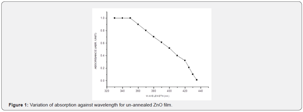
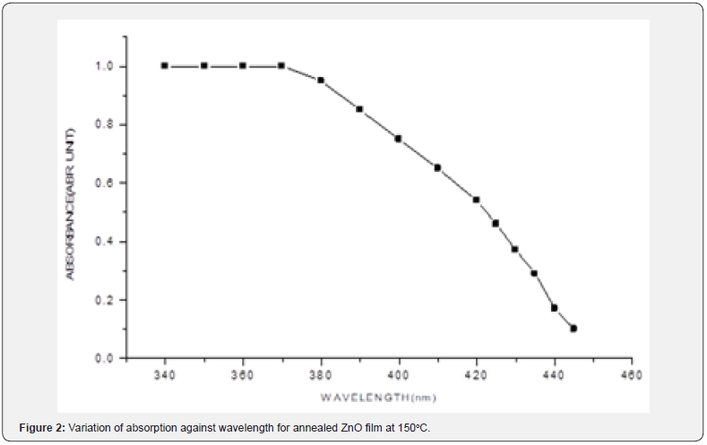
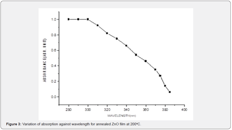
The variation of optical absorbance of ZnO layers were investigated in the 320nm to 440nm wavelength range at room temperature. Figures 1-3 shows absorption levels a selected sample form each cluster of three samples as measured by the UV-V spectrometer.
From figures 1-3 it can be noted that the absorption ratio generally decreased with increase in wavelength. In the unannealed sample in figure 1, there was a higher absorption for wavelengths from 330 - 350nm and thereafter, there was a consistent decrease in absorption. In the annealed sample at 150oC in figure 2, there was a higher absorption from 340 - 370nm wavelengths. In the annealed sample at 200oC in figure 3, there was a higher absorption from 350 - 370nm wavelengths. It can further be observed that within the wavelength range of 340 - 370nm, the sample annealed at 150oC had higher absorption ratios as compared to annealed layers at 200oC. These ratios suggest that thin films annealed at 150 are more potential for solar cell application [1,18] as compared to the latter. The ability to absorb photons for a solar energy collection layer affect negatively the efficiency of the solar cell and therefore, an attempt must be made to decrease photon absorption in ZnO films if they have to be used as solar energy collection layers. In general, the ratios obtained were comparable with those reported in literatures [10-12]. Transmittance was measured within the 200nm to 800nm wavelengths at room temperature and the variation of transmittance was as shown in figures 4-6.
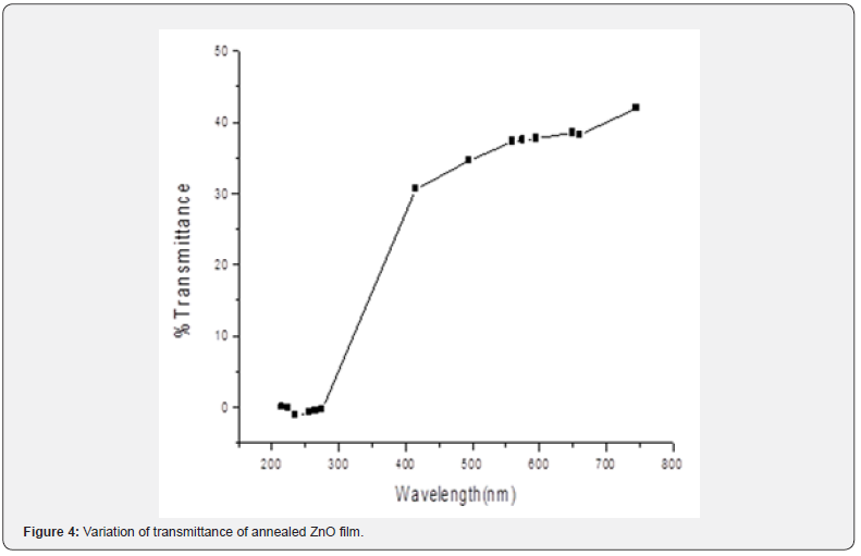
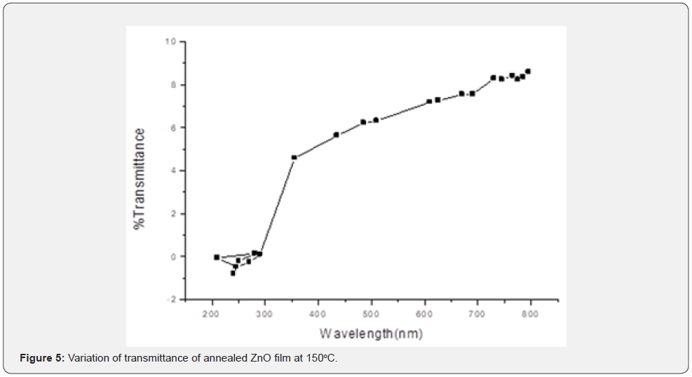
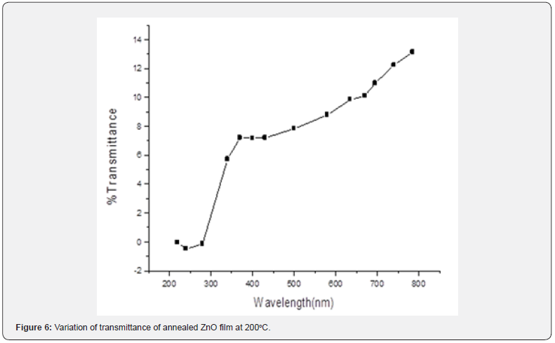
The unannealed films showed a transmittance of about 43.1% at 780nm. The annealed sample at 150oC exhibited 9.1% at 795nm while those annealed at 200oC registered 13.4 % at 784.9nm wavelengths. It can be noticed that transmittance increased with increase in wavelength. It reaches very high ratios in the NIR solar spectral region. Such high values suggest that the ZnO films are potential as solar photon collection layer [19,20] in photovoltaic cell applications. The unannealed films exhibited a higher transmittance 43 % at wavelength 780 nm showing that the unannealed films have a potential use in photovoltaic cell applications as compared to annealed samples. They will reduce photon reflection and increase radiation transmission to the photon collector fluid. The ability to transmit photons for a solar energy collection layer affect positively the efficiency of the solar cell and therefore, an attempt must be made to increase photon transmission in ZnO films if they have to be used as solar energy collection layers. Similar findings here are comparable with available literature Samir and Riyam, (2013) [16] and Sandeep and Dhananjaya, (2012) who hold a similar view that they are suitable [9,21] for solar energy collection.
Band gap energy
The average band gaps were obtained through simulation and calculation using their absorption coefficient, absorbance and thickness and summarized in table 2.

Table 2 shows that the unannealed films had a band gap of 3.08eV while the annealed at 150oC and 200oC has a band gap of 3.19eV and 2.86eV. These values will be within range in a literature by Jamil et al. [16], Benramache et al. [15] and Nagarani &Vasu [22]. Thickness forms a core parameter in solar cells. In most inorganic thin films, when their thickness gets smaller to values below 15.0nm [13], their band gap values increase with decreases in thickness. Further, the band gap can even become larger than the band gap of its bulk material [9] if its thickness falls below less 10nm. This becomes a clear indicator to show that there occurs a band gap expansion. Therefore, band gap increases with film thickness increase and this is because the film behaves as the bulk material. This reduction in the band gap energy, due to the thickness increment, is attributed to the quantum confinement effect.
Fourier transform infrared spectroscopy
In FTIR, infrared photons get absorbed by a thin film while some get transmitted and passes through. FTIR transmittance analysis in the wave number range from 600cm-1 to 4000cm-1 in vestigation on solid powder at room temperature. From figures 7-9, the unannealed films registered a transmittance of 91.8508 at wave number of 600cm-1 while the annealed at 150oC recorded 94.076 at wave number of 676cm-1. The films annealed at 200oC registered 104.108 at wave number of 642cm-1.
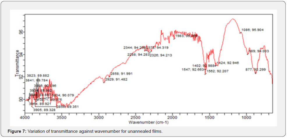
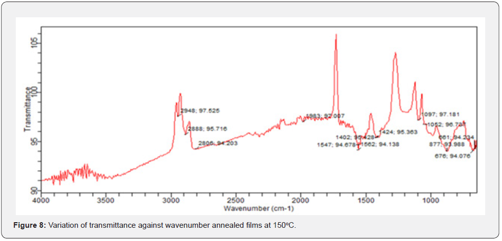
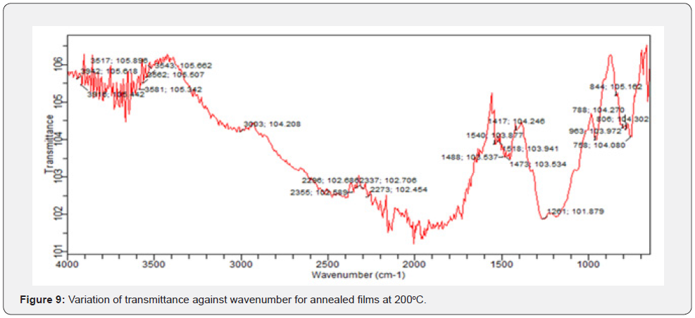
These values show a broad transmittance range per unit wave number. The unique peaks positioned at 1634.00cm-1 and 620.93cm-1 correspond to deformation vibration and stretching of the Zn-O bond. From figures 7-9, we can extract a general information on the overview of the ZnO molecular structure, its chemical environment before and after annealing, any unique orientations formed after annealing at different temperatures and even any conformations of ZnO bond structures based on their characteristic frequencies. A FTIR spectrum represents photon absorption and transmission at molecular level, and this is what creates a molecular fingerprint of specific material. Thus, there are no two unique molecular structures that can produce the same spectra in the infrared region. This suggestion agrees with Riyadh et al. [20] and Swati, Mahendra, [21]. Similarly, some literatures by Harish & Renu, [7], Jurablu et al. [17] and Ziaul et al. [23] hold the same view that ZnO have suitable transmittances [20-25] for solar cell energy collection at 420 cm-1 to 520 cm-1 wave number range [26- 29].
Conclusion
ZnO films were deposited on glass substrates using screen printing technique. Their structural and optical properties were investigated. The films were annealed at 150°C, and at 200°C while one film was unannealed but dried at ambient temperature. Thickness was calculated by estimation using the mass difference. Absorption and transmittance were measured at room temperature. The findings revealed that annealed ZnO films at 150°C exhibited higher absorptions for 340-370nm wavelengths as compared to those annealed at 200°C at 350-370nm wavelength range. These findings were found to be appropriate for use in photovoltaic cell applications as it was evident that with higher quality ZnO nanomaterial films, the future for ZnO as a solar energy collection film was going to be very fascinating. The results suggested that the properties of ZnO were very promising for the advancement of current levels in nanorod Sensors, Spintronics, and in the developments on Piezoelectricity sources.
References
- Mao Y, Li Y, Zou Y, Shen X, Zhu L, et al. (2018) Solvothermal synthesis and photocatalytic properties of ZnO micro/nanostructures. Ceramics International 45(2): 1724-1729.
- Lincot D (2010) Solution growth of functional zinc oxide films and nanostructures. MRS bulletin 35(10): 778-789.
- Wai HS, Li C (2022) Effect of Aluminum Doping Ratios on the Properties of Aluminum-Doped Zinc Oxide Films Deposited by Mist Chemical Vapor Deposition Method Applying for Photocatalysis. Nanomaterials 12(2): 195.
- Fayaz RH, Rozati SM (2022) Synthesis and investigating effect of tellurium-doping on physical properties of zinc oxide thin films by spray pyrolysis technique. Applied Physics A 128(3): 1-8.
- Khiari M, Gilliot M, Lejeune M, Lazar F, Hadjadj A (2022) Preparation of Very Thin Zinc Oxide Films by Liquid Deposition Process: Review of Key Processing Parameters. Coatings 12(1): 65.
- Amari R, Mahroug A, Boukhari A, Deghfel B, Selmi N (2018) Structural, Optical and Luminescence Properties of ZnO Thin Films Prepared by Sol-Gel Spin-Coating Method: Effect of Precursor Concentration. Chin Phys Lett 35(1): 016801.
- Harish K, Renu R (2013) Structural and Optical Characterization of ZnO Nanoparticles Synthesized by Microemulsion Route. International Letters of Chemistry, Physics and Astronomy 14: 26-36.
- Parihar V, Raja M, Paulose R (2018) A brief review of structural, electrical and electrochemical properties of zinc oxide nanoparticles. Rev Adv Mater Sci 53: 119-130.
- Surya PG (2012) Synthesis and Characterization of Zinc Oxide Nanoparticles by Sol-Gel Process. Al - Qadisiya Journal for Engineering Sciences 7: 31.
- Tsai SY, Lu YM, Lu JJ, Hon MH (2006) Comparison with electrical and optical properties of zinc oxide films deposited on the glass and PET substrates. Surface and Coatings Technology 200(10): 3241-3244.
- Wai HS, Li C (2022) Effect of Aluminum Doping Ratios on the Properties of Aluminum-Doped Zinc Oxide Films Deposited by Mist Chemical Vapor Deposition Method Applying for Photocatalysis. Nanomaterials 12(2): 195.
- Bushra KH, Al Maiyaly IH, Ayser JI (2014) Effect Ambient Oxidation on Structural and Optical Properties of Copper Oxide Thin films. International Journal of Innovative Research in Science, Engineering and Technology 3.
- Goswami M, Adhikary NC, Bhattacharjee S (2017) Effect of annealing temperatures on the structural and optical properties of Zinc Oxide nanoparticles prepared by chemical precipitation method. Optik - International Journal for Light and Electron Optics 158: 1006-1015.
- Kaushik S, Pandey S, Singhal R (2022) Effect of Annealing on Morphological, Structural and Electrical Characteristics of Zinc Oxide Layer for RRAM Applications. ECS Journal of Solid-State Science and Technology 11(3): 035003.
- Benramache S, Boubaker B, Hamza B (2013) Preparation of transparent Conductive ZnO:Co and ZnO:In thin films by ultrasonic spray method. Journal Of Nanostructure in Chemistry 5: 542.
- Jamil NY, Najim SA, Muhammed AM, Rogoz VM (2014) Preparation, Structural and Optical Characterization of ZnO/Ag Thin Film by CVD. Physics DeP College of Science, Mosul Univ Mosul, Iraq Sumy State University, 2, Rimsky-Korsakov, Ukraine 3(2).
- Jurablu S, Farahmandjou M, Firoozabadi TP (2015) Sol-Gel Synthesis of Zinc Oxide (ZnO) Nanoparticles: Study of Structural and Optical Properties. Journal of Sciences, Islamic Republic of Iran 26, 3: 281-285.
- Obeid MM, Jappor HR, Al Marzoki K, Al Hydary IA, Edrees SJ, et al. (2019) Unraveling the effect of Gd doping on the structural, optical, and magnetic properties of ZnO based diluted magnetic semiconductor nanorods. RSC 9: 33207.
- Parangusan H, Ponnamma D, Al-Maadeed MA (2019) Effect of cerium doping on the optical and photocatalytic properties of ZnO nanoflowers. Bull Mater Sci, Indian Academy of Sciences.
- Riyadh MA, Quraish AK, Kassim MS, Rawaa AA, Roaa JM, et al. (2015) Synthesis of Zinc Oxide Nanoparticles via Sol - Gel Route and Their Characterization. Journal of Nanoscience and Nanotechnology 5(1): 1-6.
- Swati SK, Mahendra DS (2015) Optical and Structural Properties of Zinc Oxide Nanoparticles. International Journal of Advanced Research in Physical Science (IJARPS) 2: 14-18.
- Nagarani N, Vasu V (2013) Structural and Optical Characterization of ZnO thin films by Sol- Gel Method. Journal on Photonics and Spintronics 2(2).
- Ziaul RK, Mohd SK, Mohammad Z, Khan MS (2011) Optical and Structural Properties of ZnO Thin Films Fabricated by Sol-Gel Method. Journal of Materials Sciences and Applications 2(5): 340-345.
- Attaf A, Djadai A, Derbali A, Saidi H, Aida MS, et al. (2022) The effect of ultrasonic wave amplitude on the physical properties of zinc oxide (ZnO) deposited by ultrasonic spray method. Materials Science and Engineering: B 275: 115525.
- Li H, Wang J, Liu H, Yang C, Xu H, et al. (2004) Sol-gel preparation of transparent zinc oxide films with highly preferential crystal orientation. Vacuum 77(1): 57-62.
- Oluyamo SS, Nyagba MS, Ojo Ambrose S (2014) Optical Properties of Copper (I) Oxide Thin Films Synthesized by Silar Technique Iosr. Journal of Applied Physics (Iosr-Jap) 6: 102-105.
- Samir HA, Riyam IJ (2013) Study the Optical Properties of Copper Oxide Thin Film Deposited by Cold Spray. Al - Qadisiya Journal for Engineering Sciences 6(4).
- Sandeep S, Dhananjaya K (2012) Effect of Annealing Temperature on the Structural and Optical Properties of Zinc Oxide (ZnO) Thin Films Prepared by Spin Coating Process. Department of Sciences, Manipal University, Manipal-576 104, Karnataka, INDIA. International Conference on Materials Science and Technology (ICMST 2012).
- Soni A, Bhamu KC, Sahariya J (2019) Investigating effect of strain on electronic and optical properties of lead-free double perovskite Cs2AgInCl6 solar cell compound: A first principle calculation. Journal of Alloys and Compounds 817.


