


Influence of Donated Pair of Electrons by a Nitrito-Group Ligand on the Solid-State Properties of Lead Sulfide Thick Films
Mosiori Cliff Orori*
Department of Mathematics and Physics, Technical University of Mombasa, Kenya
Submitted: December 29, 2022; Published: January 27, 2023
*Corresponding author: Mosiori Cliff Orori, Department of Mathematics and Physics, School of Applied and Health Sciences, Technical University of Mombasa, Mombasa, Kenya
How to cite this article: Mosiori Cliff O. Influence of Donated Pair of Electrons by a Nitrito-Group Ligand on the Solid-State Properties of Lead Sulfide Thick Films. JOJ Material Sci. 2023; 7(3): 555715. DOI:10.19080/JOJMS.2023.07.555715
Abstract
In general, thick and thin films are developed to provide special properties that range from electrical properties, optical, mechanical and chemical properties that can satisfy the needs for specific applications in technology. Lead sulfide (PbS) is an example of such films. Lead sulfide thin films have been synthesized on glass substrates. Some of the advantages of PbS thin film in olar cell applications include low material consumption, shorter energy payback period, large area modules, monolithic integration, tuneable material properties, low-temperature processes, and transparent modules. PbS thin films help also help in preventing corrosion of metallic parts of many devices. They are also used to offer protection against wear in moving parts. Materials such as jewelry, wrist watches, and knives are often coated to avoid corrosion. For deposition of PbS thin films, lead acetate is used as lead precursor and for sulfur source thiourea, has been was used in many studies.in this study, three samples of lead sulphide thick films were deposited on microscope glass slides at varying nitrito-group ligand concentrations at room temperature using solution method. The nitrito group ligand has a capacity to coordinate a central metal {Pb) atom using two different sites. First, it can use the nitrogen (N) atom as donor atom (nitrito group) and the oxygen (O) as donor atom (nitrito group). Secondly, it can use a sulphur (S) atom as donor atom ( in a thiocyanate group) and nitrogen (N) atom as donor atom ( as in a isothiocyanate). The influence of nitrito-group ligand on the solid-State properties of PbS thin films deposited by chemical bath technique were investigated and characterized using UV-VIS spectrophotometer and Four-Point Probe (FPP) technique. They were analyzed graphically, and the results show that, the donated pair of electrons from the nitrito group ligand caused absorption edge to decreases towards longer wavelength region while band gap energy increase from 1.61eV to 3.71eV with increase concentration. On the sampled films, there was a consistent increase in the sheet resistance and electrical conductivity as the concentration of Nitrito-group ligand increases.
Keywords: Lead sulphide; Nitrito-group ligand; Solid state Properties; Solution technique
Introduction
A nitrito group is known to be an ion or molecule that is able to donates a pair of electrons to the central metal atom or ion to form a coordination complex [1]. Nitrito groups can be anions, cations, and neutral molecules as long as it is capable of acting as a Lewis bases (it can donate pairs of electrons) and cause a central metal atom to act as Lewis acid (it can acceptor pairs of electron). During this pair of donor-acceptor interactions, the nature of bonding between central metal atoms to the nitrito-group ligand may vary from being an ionic bond to a covalent bond. In this regard, a nitrito-group can be cations (NO+, OH-, NH2– and N2H5+), anionic nitrito group (electron-pair acceptors like CN–, NCS–,) or neutral nitrito-group (like H2O, CO and NH3) [2]. It all depends on the number of binding sites present within the central metal atom which also varies with its resulting charge and particle size. Several chalcogenide compounds [3] with unique properties have attracted great attention for solid state device applications. They have shown potential multipurpose applications especially for devices that require a perovkite structure that couple well with either gas-solid interface or heterogeneous catalytic nature. These chalcogenide compounds are easy synthesizing [4], easily to vary their chemical and physical properties for specific ad unique applications.
Lead sulphide is a chalcogenide semiconductor material [5]. It has attracted a great research interest in the recent past for various reasons. It has unique properties, readily available in abundance, has excellent structural, optical and electrical properties that can be manipulated for specific technological applications [6]. Therefore, lead chalcogenide materials have excellent absorption coefficients and appropriate suitable band gaps capable to absorb photons from natural sun light. They have attracted particular interest in large area fabrication of solar selective coatings, photodiode arrays, photoconductors, sensors and solar cell [7]. Several deposition techniques have been used to growth binary chalcogenide [8] among them being CBD which was used PbS in this study and whose results is presented for which its optical properties are reported within UV, Visible, and near infrared region (NIR) of radiation. Mathematical approaches were also used analyze its optical properties in order compare the experimental and theoretical analysis in related studies elsewhere [5,9-13]. This study examined the influence of a pair of electrons from a nitrito-group ligand on the optical properties of binary PbS thin films grown by solution technique.
Theory
Lead sulfide also known as galena is a binary chalcogenide with PbS as its chemical formula with a molecular weight of 239.30 [11]. It has a Fm3m symmetry with a lattice constant of 5.936 Å, a very narrow band gap of 0.37eV, a magnetic susceptibility of - 0.0000836 that influence an electron and hole mobility of 600 cm2/Vs in each particle. Lead sulfide exhibits very attractive thermal properties that include heats of fusion and formation of 72J/g, and 435kJ/mole respectively with a thermal conductivity of 2.30 W/mK [14]. It also exhibits a density of 7.61 g/cm3 with a Mohs hardness of 2.5 at a refractive index is 3.91. Lead (II) sulfide has a cubic crystal structure with unit cells formed by one anion surrounded by some 6 cations as shown in figure 1.
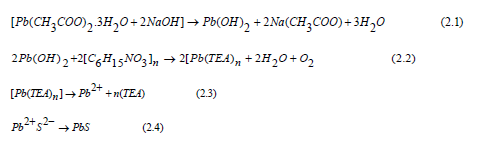
Lead sulfide can be formed by reacting a cation of Pb+2 from a solution and the anion of S-2 from another aqueous solution as illustrated below using lead acetate [15].
Lead sulfide has been under investigation as a semiconductor for many years. It is a toxic semiconductor only if it gets decomposed by heat to generate lead oxide and sulfur oxide products. Lead sulfide has found itself as a potential material for applications in infrared detectors [10], many photo-optic applications and even as a slip-property modifier commonly used in the friction industry to enhance heat conduction and regulate friction coefficients [16] in moving parts that are in contact in most automobile industrial applications.
Methodology
Reagents and chemicals
The following reagents were used: a soap solution, acetone, methanol, de-ionized water, distilled water, sodium hydroxide, lead acetate trihydrate, thiourea, and tri-ethanolamine among others.
Apparatus and materials
The following materials: cotton wool, glass slide substrates, digital PH meter, furnace, digital stop clock, magnetic stirrer, retort stand and clip, beaker and aluminum foil among others.
Cleaning of substrates
Glass slide substrates were first scrubbed thoroughly with a wet cleaned cotton wool in soap solution from a few second. I was then rinsed with running distilled water. They were again ultrasonicate in a bath of acetone, followed by methanol and finally rinsed again in distilled water at room temperature for few hours. After drying, they were rinsed with de-ionized water and dried in an open furnace at moderate temperature for a few minutes. They were then stored.
Experimental procedures
Solution technique was employed in this study. A 2.5ml of 0.5 Mole of lead acetate trihydrate, about 2.5ml of 2.0 mole of sodium hydroxide were mixed and thoroughly stirred. Some 3.0ml of 1.0 mole of thiourea was added. Three different concentrations of tri-ethanolamine (Nitrito-group ligand) was prepared at 25.6oC (room temperature in the laboratory at the experimental time) as to varied from 0.2 moles labeled X, 0.4 moles labeled Y to 0.6 moles labeled Z. To obtain a volume to submerge the glass slide (substrate), some distilled water was added to make the total volume of 80ml in a 100ml beaker and covered with an aluminum foil to prevent unwanted particles land in the bath. A digital PH meter was used to determine the PH of the solution which was maintained at 11. A magnetic stirrer was used for 10 minutes to ensure homogeneity in the bath solution. The glass substrate was vertically clamped using retort stand and clip over the beaker and gently lowered into the reaction bath and allowed to stand still for 18 hours separately as X, Y and Z samples in TEA concentration of 0.2M, 0.4M and 0.6M respectively. After 18 hours according to Abbass et al. (2022), the three samples were gently and slowly pulled out of the bath, rinsed in distilled water before drying them slowly in an open furnace at 30oC.
Film characterization

Solid state properties were characterized using UV-VIS Spectrophotometer over a spectra ranging between (200 - 1000nm) to determine transmittance, absorbance, extinction and absorption coefficients, skin depth, band gap and Urbach energies, refractive and dielectric constant.
Results and Discussion
The process of drying the thin films in an open furnace at room temperature was to remove the residual water and any other adsorbed surface impurities that may have been present. The thin films obtained were observed to be well adhered to the glass substrates and were very homogeneous over the coated surfaces. The deposited films were characterized using various characterization techniques that included using the UVVIS spectrophotometer to determine the optical and solid-state properties.
Skin depth
Figure 2 shows the variation of penetration depth of the incident photon energy on the X, Y and Z samples where it can be observed that the depth decreases as incident photon energy increases.

Further, penetration depth of sample X increases with the photon energy until it reaches a point of about 1.800eV where it loses absorption power. Its light wave amplitude reduces to a point where it can be regarded as it’s called cut-off wavelength [11] where transmittance for X is lower than that of Y (at 2.42eV) and that of Z (at 4.21eV). Here, transmittance for Z is the highest. Since a Nitrito group ligand donates a pair of electrons, these electrons then increase the skin depth of PbS thin films. Similarly, the skin depth increases as we increase the concentration of Nitrito group ligand or as the number of donated pair of electrons increases. Therefore, penetration depth can be attributed to the decrease observed in the film thickness as the Nitrito-group concentration increases. Thus, skin depth in PbS thin films can be determined by the mount of electron pair donated by a Nitrito-group ligand. According to literature [12] the skin depth of any material is a measure of the maximum distance for a certain electromagnetic radiation is able penetrate before it is complete absorption by the atoms of the material [7]. This implies that penetration depth is absorption coefficient dependent.
Transmittance and absorbance
Transmittance was measured within the spectra range of 200 - 1000nm and the spectra data was used to plot transmittance against wavelength as shown in figure 3 while figure 4 shows the calculated absorbance spectra of the PbS thin films.

As shown in figure 3, it can be deduced that there was zero radiation transmission between 200 - 620nm wavelengths for both samples X and Y. After 620nm, it increased exponentially with wavelength due to the lower amounts of pair of electrons donated in each instant. The consequence was an increased film thickness. Due to the donated pair of electrons, sample Z has an excellent transmittance of about 50% that can be attributed to the large number of electron pairs available in the precursor solution in the bath. A similar transmittance spectrum for PbS thin films that attributed to the thickness of the films was obtained by Abbas et al. 2011 where it was concluded that a ligand donates a pair of electrons that influence an increase in optical transmission in thin films. This was an amazing property that makes PbS films with dimensions of sample Z suitable for antireflection coatings and even solar flat-plat collector applications [4]. The curve in figure 4 is a graph of the absorbance plotted against the spectra wavelength and it can be deduced that sample X had a higher absorption as compared to sample Y. in fact, there was zero absorption for both sample Y within the spectra range of 200 - 550nm and for sample X in the range of 200 - 700nm. This was attributed to the donated electron pair concentration as this has been deduced to influence thickness of PbS films elsewhere [15]. It can also be deduced from figure 4 that absorption for samples X and Y increase with decreases in wavelength while sample Z has the lowest absorption because it had the highest concentration of pairs of donated electrons and that caused Bathocromic effect [17]. Its absorption edge Red- shifted (towards longer wavelength) which was attributed to decrease in the direct band gap. Similar observations were made by [2].

Refractive index (n)
Figure 5 shows a plot of refractive index as a function of photon energy for PbS thick films. As deduced from figure 5, samples X and Y had a refractive index of about 1.810 within the visible spectra that was attributed to the number of electron-pair donated by the Nitroto-group ligand. This pair of electrons is responsible for the increase the thickness of PbS films. Similarly, sample Z, exhibited the lowest refractive index far below 0.821 in the UV region which was attributed to narrower thickness as compared to X and Y. Equally, the pair of donated electrons from the Nitroto-group played a key role. It was concluded that the scattering of photons within this small or narrow thickness can be ascribed to the smaller and uniform grain distribution present in sample Z and therefore, it can be deduced that, increasing the concentration of Nitrito group ligand during film deposition of PbS thick films influences a decrease in refractive index within the ultraviolet spectrum. Therefore, refractive index is the rate at which photons are slowed down as they propagate through an optical active material [18] and therefore, form one of the most significant optical properties to be considered whenever any optical material is to be chosen for any optoelectronic application.

Frequency response
Figure 6 shows the frequency response of PbS thick films against the photon energy. From figure 6, these thick films exhibited higher frequency in which it can be deduced that sample X had the highest frequency response as compared to sample Y that was slightly lower. However, sample Z exhibited the lowest frequency response. It can be deduced that the frequency response of these thick films exhibited a similar trend as compared to its refractive index. Since frequency response is a measure of optical conductivity of a material on irradiation with electromagnetic radiation, it was noted that it was strictly dependent only on absorption coefficient and refractive index. However, the values of optical conductivity seemed to decrease sequentially as the number of donated pair of electrons form the Nitrito group ligand increases. Sample X with the lowest concentration of pair of donated electrons responded quickly and sharply to the frequency of the incident photon as compared to sample Y and sample Z respectively. It was concluded from the sight of the pair of donated electrons from the Nitrito group ligand that the number of donated pair of electrons decreases the optical conductivity of PbS thin films.

Molar absorptivity and absorption edge
Figure 7 shows a variation of optical absorption coefficient while figure 8 shows a plot of extinction coefficient as a function of wavelength within the 200 - 1000nm solar spectra range. From figure 7, it can be observed that the films in sample X and sample Y which were with lower number of donated pair of electrons were thicker compared to sample Z which was thinner. Similarly, sample X and sample Y showed zero photon absorption within 200 – 520nm wavelength spectra and exhibited absorption edges at 542nm and 653nm wavelength for sample X and sample Y respectively. However, sample Z had the highest optical absorption coefficient in the UV-VIS region which was attributed to the number of pairs of electrons donated by the Nitrito-group ligand. Equally, the exhibited absorption coefficient increases as incident radiation shifted towards longer wavelength with higher values in the band absorption region. Therefore, an increase in absorption coefficient leads to an increase in electron transition in the energy bands which influences a reduction in the band gap energy of the thick films [12,13]. According to Priyanka, and Naik, (2022), absorption coefficient of PbS films corresponds to the transition of electrons or the excitation of electrons from a valence band to the conduction band of the crystals. This is a component that is employed to determine the nature of the optical band gap. From figure 8 shows, it can be observed that within the UV region, the extinction coefficient increased with increase wavelength.
The notable increase occurs at wavelengths below 706nm, 551nm and 353nm for samples X, Y and Z respectively. This increase was attributed to the high photon absorption due to the smoothness of the surface of the films. It can be deduced that an increase in the number of donated pair of electrons from the Nitrito-group ligand decreased the extinction coefficient right from the absorption edge towards and within the visible region. Therefore, absorption coefficient in PbS thick films was significantly slightly constant within the visible range especially in the wavelengths above 910nm though all the samples exhibited a dominant peak around 800nm wavelength. It therefore true that, extinction coefficient is a characteristic material property that may determine how a material absorbs, transmits or reflects light or photons at a particular wavelength [8,14]. It is therefore an intrinsic material property that can isolate an atomic, chemical, and protein structural composition. Molar absorptivity [9] is true a measure of photon or light loss takes place due to photon scattering and absorption per unit volume of a material.


Band gap energy
Figure 9 shows the variation of estimated using Tauc plot against the photon energy while figure 10 shows the variation band energy gap as a function of nitroto-group for sample X, Y and Z of PbS thin films estimated by extrapolation of the linear portion of each Tauc plot to the photon energy axis at a point where the term is arbitral zero.


From figures 9 & 10 respectively, it is observed that band gap energy reduces linearly with the photon energy. Band gap also narrows down as Nitrito-group ligand that donates pairs of electron increases. This implies that after a certain limiting size of particle size which is associated with the excition radius determines the space between the band levels of the material changed. The Nitrito-group ligand reduces the band gap energy and for samples X, Y and Z, it was reduced to a range of 0.4 - 0.6eV respectively which resulted into values close to Abbas et al. [15] and this may be due to the nanocrystalline nature of PbS as a material. This trend was attributed to the effect of quantum confinement [4]. Sample X was then recommended as a good material for solar cell fabrication and in accordance with theory [3], samples had a direct band gap by estimation.
Urbach energy
A plot of as a function of the photon energy was determined by taking the reciprocal of the slope and is presented in figure 12.
From figure 11, it was observed that the values of Urbach energy increased as the of Nitrito group ligand concentration increase. The increase was attributed to an increase of the defects in the thick film. It also implies that there exists a localized state in the energy band gap [9]. Urbach energy therefore represents the degree of disorder and defects [12] and it corresponds to the band tail width of the localized states in the energy gap [7].


Dielectric constant (ε)
Both the real and imaginary dielectric constants were plotted in figures 12 & 13 for wavelength between 300nm - 900nm.
As compared to the refractive index curve, all samples exhibited a similar trend. This suggested that square of their respective absorption coefficient values were much smaller compared to the square of their corresponding refractive indexes showing that dielectric constant depend on refractive index though the average value of the real dielectric constant is considerably greater than that of the imaginary part. It was also deduced that both the real and imaginary dielectric constant decreases as the concentration of Nitrito group ligand concentration increased.
Similarly, dielectric constants increased with decrease in incident radiation wavelength and this implied that both dielectric constants decrease with a decrease in the amount of electron pairs donated. As seen in figure 13, the oscillatory behavior of the imaginary dielectric constant appears mainly in the transparent region. However, at the absorption edge, a sharp increase in the imaginary dielectric constant is noted with increase in photon energy. The permittivity of a material represents the ability of a material to concentrate electrostatic lines of flux due to static charges. It actually represents the ability of a material to store electrical energy whenever there is an electric field [8]. Therefore, the real and imaginary part of dielectric constant purely depends on refractive index and absorption coefficient [19,20].

Conclusion
The influence of a pair of donated electrons from nitritogroup ligand was investigated using grown by solution technique. It was observed that the pair of donated electrons caused a slight variation in some of the optical properties PbS thick films. The following optical properties were noted to influence by the pair of donated electrons: refractive index, real and imaginary dielectric constant, band gap energy and Urbach energy. Specifically, the band gap slightly widened which was a clear indication of a variation of grain sizes and defect levels in the samples analyzed. The films were recommended for wider band application as compared to the theoretical PbS thick film band gap.
References
- Priyanka P, Das S, Naik (2022) Various Optoelectronic Properties for Different Applications. Engineering and Technology Journal.
- Fouda AN, Marzook M, Abd El Khalek HM, Ahmed S, et al. (2016) Structural and Optical Characterization of Chemically Deposited PbS Thin Films. Silicon 9: 809-816.
- Sun Y, Gao H, Wu S, Duan Y, Qian M, et al. (2022) The influence of device structure on resistance switching in PbS QDs film inserted RRAM. Applied Physics Letters 121(3): 032104.
- Taghipour N, Tanriover I, Dalmases M, Whitworth GL, Graham C, et al. (2022) Ultra‐Thin Infrared Optical Gain Medium and Optically Pumped Stimulated Emission in PbS Colloidal Quantum Dot LEDs. Advanced Functional Materials 32(27): 2200832.
- Wang Y, Lin DH, Luo SH, Zhang X, Fu C, et al. (2022) Ultraviolet Photodetectors Based on Nanometer-Thick Films of the Narrow Band Gap Semiconductor PbS. ACS Applied Nano Materials 5(7): 8894-8901.
- Thangaraju B, Kaliannan P (2000) Spray pyrolytically deposited PbS thin films. Semiconductor science and technology 15(8): 849.
- Aynehband S, Mohammadi M, Poushimin R, Azar MH, Nunzi JM, et al. (2022) Self-assembly, stability, and photoresponse of PbS quantum dot films capped with mixed halide perovskite ligands. Materials Research Bulletin 147: 111648.
- Yang Y, Rao Z, Xu Q, Liang Y, Yang L (2022) Improving the photovoltaic performance for PbS QD thin film solar cells through interface engineering. Journal of Colloid and Interface Science 627: 562-568.
- Busari RA, Taleatu BA, Adewinbi SA, Adewumi OE, Omotoso E, et al. (2020) Synthesis and surface characterization of electrodeposited quaternary chalcogenide Cu2ZnxSnyS1+x+2 y thin film as transparent contact electrode. Bull Mater Sci 43: 83.
- Duff M, Bae S, Lee JK (2022) Characterization of carrier transport using a bifacial structure for rational design of p-n junction PbS solar cells. Journal of Power Sources 518: 230742.
- Albaladejo SM, Becker KD, Baird EC, Hofstetter YJ, Carwithen BP, et al. (2022) Interdot Lead Halide Excess Management in PbS Quantum Dot Solar Cells. Advanced Energy Materials 12(45): 2202994.
- Chehaibou B, Izquierdo E, Chu A, Abadie C, Cavallo M, et al. (2022). The complex optical index of PbS nanocrystal thin films and their use for short wave infrared sensor design. Nanoscale 14(7): 2711-2721.
- Sloboda T, Svanström S, Johansson FO, Bryngelsson E, García FA, et al. (2022) The impact of chemical composition of halide surface ligands on the electronic structure and stability of lead sulfide quantum dot materials. Physical Chemistry Chemical Physics 24: 12645-12657.
- Liu X, Fu T, Liu J, Wang Y, Jia Y, et al. (2022) Solution Annealing Induces Surface Chemical Reconstruction for High-Efficiency PbS Quantum Dot Solar Cells. ACS Applied Materials & Interfaces 14(12): 14274-14283.
- Abbas MM, Shehab A AbM, Al Samuraee AK, Hassan NA (2011) Effect of Deposition Time on the Optical Characteristics of Chemically Deposited Nanostructure PbS Thin Films. Energy Procedia 6: 241-250.
- García WRM, Herrera MAL, García GL, Martínez CL, Caballero BF, et al. (2022) Structure, morphology, and local photoelectrical characterization of PbS films grown by SILAR. Materials Letters 314: 131844.
- McDonald SA, Konstantatos G, Zhang S, Cyr PW, Klem EJ, et al. (2005) Solution-processed PbS quantum dot infrared photodetectors and photovoltaics. Nature materials 4(2): 138-142.
- Liu Y, Wu H, Shi G, Li Y, Gao Y, et al. (2022) Merging Passivation in Synthesis Enabling the Lowest Open‐Circuit Voltage Loss for PbS Quantum Dot Solar Cells. Advanced Materials 2207293.
- Soonmin H, Paulraj I, Kumar M, Sonker RK, Nandi P (2022) Recent Developments on the Properties of Chalcogenide Thin Film.
- Wang Y, Liu Z, Huo N, Li F, Gu M, et al. (2019) Room-temperature direct synthesis of semi-conductive PbS nanocrystal inks for optoelectronic applications. Nature communications 10(1): 1-8.