The Morphological Properties of Zns Nanoparticles Deposited on Glass Substrates as a Function of Aluminum Content
A A Ahmed* and M D Abd Alla
Department of Physics, College of Science, Sudan University of Science and Technology (SUST), Sudan
Submitted: September 01, 2022; Published: November 04, 2022
*Corresponding author: A A Ahmed, Department of Physics, College of Science, Sudan University of Science and Technology (SUST), Sudan
How to cite this article: A A Ahmed, M D Abd A. The Morphological Properties of Zns Nanoparticles Deposited on Glass Substrates as a Function of Aluminum Content. JOJ Material Sci. 2022; 7(2): 555708. DOI:10.19080/JOJMS.2022.07.555708
Abstract
The pulsed-laser deposition (PLD) method was used to deposit undoped zinc sulphide (ZnS) and Al-doped zinc sulphide (AZS) films on glass substrates (GSs). The aluminum content in the ZnS films varied from 0% to 8%. The film morphology was studied using atomic force microscopy (AFM). The films were optically characterized using an Ultraviolet–Visible-near-infrared (UV-VIS-NIR) spectrophotometer with photon wavelengths ranging from 300 to 600nm. The average roughness (Sa), root-mean square (RMS) roughness (Sq), surface skewness (Ssk), and surface kurtosis (Suk) parameters of the samples were determined using the AFM method. The samples’ AFM grain sizes were found to be 4.89 nm, 5.65 nm, and 12 nm, respectively. The doped ZnS thin film’s surface roughness was found to be greater than the undoped ZnS thin film’s. The samples showed a high transmittance across the whole visible spectrum, according to the UV data. The film optical refractive-index (n) and the extinction-coefficient (k) was computed using UV–VIS spectroscopy data. The techniques used in these investigations have been described and explained in detail. Good agreement was found when comparing results from this work against previously published data.
Keywords: Thin film; PLD; AFM; UV; Surface roughness
Abbreviations: The Pulsed-Laser Deposition; AZS: Al-Doped Zinc Sulphide, GSs: Glass Substrates; AFM: Atomic Force Microscopy; UV-VIS-NIR: Ultraviolet–Visible-Near-Infrared; RMS: Root-Mean Square; Ssk: Surface Skewness; Suk: Surface Kurtosis
Introduction
The metal chalcogenide in their crystalline state possesses many outstanding properties and has attracted considerable attention in the literature [1]. Semiconductor nanoparticles (SCNPs) films made of II-VI compounds have distinct properties that make them suited to several devices and applications [2]. Tin dioxide (SnO2), titanium-dioxide (TiO2), cadmium-sulphide (CdS), cadmium-tellurium (CdTe), cadmium-selenide (CdSe), zinc selenide (ZnSe), zinc-oxide (ZnO), and zinc tellurium (ZnTe) are all well-known SCNPs and well-studied in detail [3-10]. Among the SCNPs, ZnS is one in particular that has been widely used for a variety of applications. ZnS is an easily accessible, nontoxic, and environmentally safe compound with a higher direct band-gap energy (3.7 eV) [11].
ZnS is a metal chalcogenide with a high refractive index, a large band-gap energy, and a high UV-visible transmittance [12,13]. The polytypes of ZnS are cubic-zinc blende (sphalerite) and wurtzite (hexagonal) [11]. Furthermore, ZnS structures frequently crystallize in space groups (F43m) and (P63) in the cubic zincblende (ZB) phase at low temperatures, and (P63) in the hexagonal zincblende (ZB) phase at high temperatures [11]. Several research groups have attempted to dope ZnS films with elements such as In, Al, Fe, Co, Pb, Cd, Cu, Mn, Cr, Ni, Eu, Sm, and Cl throughout the growth process [14-20]. However, there have been infrequent studies on aluminum doped with ZnS films and placed on substrates [21,22]. However, aluminum doped ZnS films deposited on glass needs further investigation. Numerous deposition techniques, including sputtering, thermal evaporation, spray pyrolysis, chemical bath deposition, close-spaced evaporation, electron beam evaporation and pulsed laser deposition have been used to prepare ZnS thin films [14,23-26].
To our knowledge, only a few investigations was conducted on zinc sulphide thin films prepared via the PLD method on glass substrates. Several methods are demonstrated, but the pulsed laser deposition technique is shown to maintain the desired composition in the deposited thin films. Because the high kinetic energy of atoms and ionized particles in the laser-produced plasma, the PLD method can be used to deposit ZnS film at low temperatures [27]. This method is used to deposit materials on large surfaces under air conditions and on a variety of substrates in a well-controlled manner. Nonetheless, due to the intricate growth mechanism and method, deposition of ultrathin ZnS and AZS films via PLD remains extremely challenging. The results of these analyses, performed by utilizing the AFM method and the UV–Vis spectroscopy, have been documented.
Materials and Methods
Sample preparation
Sigma-Aldrich analytical grade reagents, chemical, and sodalime glass substrates were purchased and used without further purification in this investigation. The precursors for Al, S, and Zn were aluminum chloride hexahydrate (AlCl3.6H2O), thioacetamide (CH3CSNH2), zinc acetate dehydrate [Zn(CH3COO)2, 2H2O)], and ethylenediamine (NH2CH2CH2NH2) of analytical reagent quality. For several minutes, the zinc-acetate and ethylenediamine were mixed and agitated to obtain a clear and uniform solution. The product was then added to the zinc-acetate solution, followed by the addition of tri-sodium citrate. The resulting solution was agitated for a few minutes in each case. Following this, it was added to the previously produced thiourea solution while stirring. To obtain Al-doped ZnS (AZS) samples, the combined materials were mixed in the proper ratio and then dried. Numerous hours were spent extensively rushing the combined AZS samples. To manufacture the pellets of the thin films, a 5-ton hydraulic press was used for 3-5 minutes at room temperature.
Thus, pellets roughly 1.2cm in diameter and 0.2cm thick were produced from the given AZS sample. The glass substrates were degreased for 12 hours prior to deposition using soap water and alcohol. Following this procedure, glass substrates (GSs) were ultrasonically cleaned for 10 minutes with alcohol and deionized water. Finally, the glass slide substrate was rinsed, washed with deionized water, and air dried. PLD with a focused Q-switchedneodymium- doped yttrium aluminum garnet (Nd: Y3Al5O12) was used to deposit the ZnS and AZS films on the glass substrates (GSs) (Nd: YAG). The depositions took place at four-hour intervals.
Pulsed-laser ablation was carried out using a focused beam in TEM00 mode laser with primary and secondary harmonic outputs at 1064 and 532nm, respectively. The laser system was operated using pulses with a duration of ten nanoseconds. A pulsed laser with an energy density of 2 J/cm2 and a frequency of 6 Hz was used to irradiate the object. The thin film target spun as the laser restored across an area of approximately 0.5cm2 with a spot size of 3 mm2 and an incidence angle of 45°.
Throughout the development process, the target-substrate distance was maintained at a constant of 2.0cm. The substrate was clamped to a heated holder, and the temperature of the deposition solution was measured. Prior to heating the source, the chamber was evacuated to a pressure of 10-3 torr. The ZnS and AZS film were deposited on the GSs using 500 pulses and 100 mJ/pulse energy. The target and laser source were separated by a predetermined distance of 12.0cm. All films were of a thickness of between 200 and 250nm. However, when the films were grown using the PLD method, the deposition rate was calibrated, in order to regulate the thickness. The details concerning the set-up of the PLD method experiment have been provided elsewhere [14]. All samples were labeled as a control (ZnS/GSs or S0), the Al-doped ZnS/GSs (ZnS/ GSs: Al 4% or S1) and the (ZnS/GSs: Al 4% or S2), respectively. The sample morphology and optical properties were measured by the AFM [28] and the UV–Vis spectrophotometer [29].
Results and Discussion
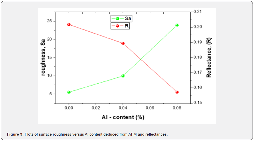
The surface roughness of the films, as defined by arithmeticmean height (Sa), root-mean square height (Sq), skew (Ssk), and kurtosis (Sku), was measured and is shown in table 1. The film arithmetic mean height was calculated to be S0 (5.509nm), S1 (9.964nm), and S2 (23.92nm), in that order. It was observed that in comparison to S0, the Sa of the sample surface increased from 5.509nm to 23.92nm with aluminum doping. The film root-mean square roughness was calculated to be S0 (7.251nm), S1 (13.30 nm), and S2 (44.11nm), in that order.

The sample skewness was found to be S0 (0.7310), S1 (1.179), and S2 (3.585), respectively. The sample kurtosis was S0 (5.046), S1 (10.38), and S2 (20.36), respectively. These findings show that the doped sample surface of S1 and S2 was rougher than the S0 surface. The dopant of ZnS/glass substrates led to a slight alteration of the parameters. However, the Sa and Sq film parameters had increased. Furthermore, the Ssk and Sku parameters of the film increased from 0.7310 to 3.585, and from 5.046 to 20.36, respectively.
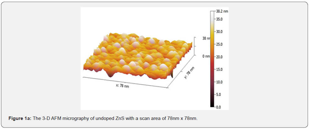
AFM micrographs of the prepared films show that spherical shape grains are uniformly distributed. Surface kurtosis values greater than 3 were found in all the examined samples, indicating sharper peaks and longer, fatter tails in general. Rku values greater than 3 indicate that the peaks and valleys have further flattened out. This finding suggests that Rsk can be used to distinguish the roughness profiles of the two surface processes. Surface roughness analysis was performed by capturing 3-D images of the surfaces of ZnS thin films with a scan area of 7.8nm x 7.8nm.
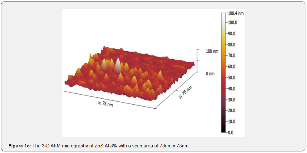
Figure 1 depicts the 7.8nm x 7.8nm 3-D images of the undoped and doped ZnS thin film surfaces for (a), (b), and (c), respectively. It is observed that Al doping induced noticeable changes in the surface morphology. The size of the grains increased for 4 wt. % Al doping (Figure 1(b)), and bigger clusters were formed on the film surface for 8 wt. % a Al doping, as shown in figure 1(c). It was also reported that Al doping in ZnS led to an increase in the grain growth.


The scales of the Z-axis in figures 1a-1c show that the surface of the undoped deposited ZnS thin film is much flatter, in comparison with the surface of the doped deposited ZnS thin film (c). When the aluminum content is gradually increased, the scales of the Z-axis of the undoped deposited ZnS thin film surface increases. It is seen in figures 1a-1c that the scales of the Z-axis are different. Figure 2 depicts a histogram of the percentages of ZnS and ZnS: Al as a function of grain size (a to c). The AFM analysis extracts surface parameters from the AZS thin films, allowing for the investigation of the surface analysis with numerical data.
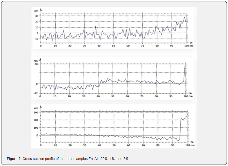
The profiles of the AFM image cross section are shown in figure 2. The AFM image cross-section shows that islands in samples grown with aluminum concentrations of 0%, 4%, and 8% have a quasi-rounded shape distribution with an RMS value of 4.89nm and 5.65nm, for 0% and 4%, respectively. In contrast, for an aluminum concentration of 8%, the profiles exhibit a quasitriangular distribution of islands with an RMS value of 12nm.
The origin of the rough surface morphologies is correlated to the enhanced aluminum at a high aluminum concentration of 8%. Small ZnS islands tend to coalesce into larger ones as a result of the extra aluminum migrating on the surface. This coalescence allows for a reduction in the density of ZnS islands. Thus, 0% aluminum concentrations favor the 2D-like growth of ZnS, resulting in a wavy surface.

A quantitative optical model was employed in the calculation of the concentration-dependent reflectance of AZS structures, as detailed below. The experimental results add to our understanding of the relationship between aluminum concentrations and optical properties. A UV–Vis–NIR spectrophotometer in the 600 nm range was used to measure the optical properties of AZS thin films at room temperature. The reflectance spectrum was obtained using a UV–Vis–NIR spectrophotometer. The effects of variables on roughness were investigated using both morphological and optical responses. Table 2 shows a more detailed comparison of the films’ refractive index (n), extinction coefficient (k), reflectance (R), and surface roughness (Sa). However, as the refractive index, extinction coefficient, and reflectance of a material decrease, the value of its surface roughness increases.

In summary, we provide a correlation between Aluminum concentration and surface morphology evolutions versus the optical parameters of AZS on substrate based on the optical properties results. The results show that the high-density island structure acts to increase the scattering of the AZS surface. Changing the concentration of Al can affect the density and size of islands.
We compare the surface roughness, aluminum content, and reflectance as shown in figure 3. It is significant to note that the contribution of all surface defects and features is regarded as the primary cause of light scattering, as a result of which reflectance decreases for reflectance measurements. Finally, based on the reflectance data, we present a correlation between AZS concentration and surface morphology.


Conclusion
In summary, un-doped and Al-doped ZnS film was deposited on glass substrates using the PLD technique. The effects of aluminum concentration on the morphological and optical properties of the films were investigated using AFM and UV methods. According to the AFM studies, the film roughness changed significantly, following dopant treatment. The average roughness, rootmean square roughness, line skewness, and kurtosis of the ZnS films deposited on the glass substrates slightly increased after aluminum content-treatment. The AFM topography of doped and deposited films with aluminum content ranging from 0% to 4% revealed a surface texture with waviness.
Acknowledgement
The authors wish to thank Professor Asmiet Ramizy of the University of Unbar’s Department of Physics for providing laboratory space. The authors funded the study privately. As a result, no grant numbers or funding sources need to be declared.
Conflict of Interest
The authors declare that no conflicts of interest will arise as a result of this manuscript’s publication. This manuscript contains material that has never been published previously.
References
- Bouznit Y, Beggah Y, Boukerika A, Lahreche A, Ynineb F (2013) New co-spray way to synthesize high-quality ZnS films. Applied Surface Science 284: 936-941.
- Kumar N, Kumbhat S (2016) Essentials in Nanoscience and Nanotechnology. In: Hoboken NJ, (Edt.), John Wiley & Sons, Inc, Carbon-Based Nanomaterials, USA, pp. 189-236.
- Guan Y, Wang D, Zhou X, Sun P, Wang H, et al. (2014) Hydrothermal preparation and gas sensing properties of Zn-doped SnO2 hierarchical architectures. Sensors and Actuators B: Chemical 191: 45-52.
- Ullattil SG, Narendranath SB, Pillai SC, Periyat P (2018) Black TiO2 nanomaterials: A review of recent advances. Chemical Engineering Journal 343: 708-736.
- Kapadnis RS, Bansode SB, Supekar AT, Bhujbal PK, Kale SS, et al. (2020) Cadmium Telluride/Cadmium Sulfide Thin Films Solar Cells: A Review. ES Energy Environ 10: 3-12.
- Sanjay P, Deepa K, Madhavan J, Senthil S (2018) Synthesis and spectroscopic characterization of cdse nanoparticles for photovoltaic applications. MsE, 360: 012010.
- Alessandro R, Elisa A (2021) CdTe-Based Thin Film Solar Cells: Past, Present and Future. Energies 14(6): 1-24.
- Abbasov I, Musayev M, Huseynov J, Kostyrko M, Babayev S, et al. (2020) Photoluminescence spectra of polycrystalline ZnSe in different experimental geometries. Ukrainian Journal of Physical Optics 21(2): 103-114.
- Droepenu EK, Wee BS, Chin SF, Kok KY, Maligan MF (2022) Zinc Oxide Nanoparticles Synthesis Methods and its Effect on Morphology: A Review. Biointerface Research in Applied Chemistry 12(3): 4261-4292.
- Dumitru M, Vlad Andrei A, Antoniu M, Rovena P, Sorina I, et al. (2021) Thickness Effect on Some Physical Properties of RF Sputtered ZnTe Thin Films for Potential Photovoltaic Applications. Nanomaterials 11(9): 2286.
- Liao J, Cheng S, Zhou H, Long B (2013) Al-doped ZnS thin flms for bufer layers of solar cells prepared by chemical bath deposition. IET Micro & Nano Letter 8(4): 211-214.
- Zhao Y, Wei XY, Peng NC, Wang JH, Jiang ZD (2017) Study of ZnS Nano-structures Based Electro-chemical & Photo-electro-chemical Bio-sensors for Uric- acid Detection. Sensors 17: 1235.
- Iosif DS, Florinel S, Angel TB, Ion B, Nicu B, et al. (2021) The Effect of the Deposition Method on the Structural and Optical- Properties of ZnS Thin Films. Coatings 11: 10.
- Eisa MH, Ahmed AA (2021) Structural-characterization of synthesized Al-doped-ZnS nanoparticles deposited on glass -substrate. Chalcogenide Letters 18(12): 783-789.
- Azmand A, Kafashan H (2019) Al-doped-ZnS thin-films: Physical and electro-chemical characterization. Journal of Alloys Compound 779: 301-313.
- Devi S, Devi KN, Sharma BI, Sarma HN (2014) Effect pf Mn2+ Doping on Structural, Morphological, and Optical Properties of ZnS Nanoparticles by Chemical Co-precipitation Method. Journal of Applied Physics 6(2): 6-14.
- Chang L, He XW, Chen LX, Zhang YK (2017) Mercaptophenylboronic acid-capped Mn-doped ZnS quantum dots for highly selective and sensitive fluorescence detection of glycoproteins. Sensors and Actuators B: Chemical 243: 72-77.
- Attaf A, Derbali A, Saidi H, Benamra H, MS Aida, et al. (2020) Physical properties of Pb-doped ZnS thin films prepared by ultrasonic spray technique. Physics Letters A 384(26): 126199.
- Mohammadreza N, Yang X, Gibson U, Reenaas TW (2015) Pulsed laser- ablation and deposition of ZnS: Cr. Thin Solid Films 590: 28-32.
- Bitri N, Ben BK, Ly I, Bouzouita H, Abaab M (2017) Studies of physical properties of the Al doped ZnS thin films prepared by Spray. Journal of Materials Science: Materials in Electronics 28: 734-744.
- Nagamani K, Revathi N, Prathap P, Lingappa Y, Ramakrishna RKT (2012) Al-doped ZnS layers synthesized by solution growth method. Current Applied Physics 12: 380.
- Nasir EM (2014) Surface Morphological and Structural Properties of ZnS and ZnS: Al thin films. International Journal of Innovative Research in Science. Engineering and Technology 3(1): 8114.
- Hague F, Rahman KS, Islam MA, Rashid MJ, Akhtaruzzaman M, et al. (2014) Growth Optimization of ZnS Thin-films by RF- Magnetron-Sputerring as Prospective Buffer- Layer in Thin -Film Solar Cells. Chalcogenide Letters 11(4): 189-197.
- Ben KY, Benhaya A, Aida MS (2015) ZnS Thin-Films Deposition by Thermal-Evaporation for Photo-Voltaic Applications. Journal of Semiconductors 36(10): 103001.
- Djelloul A, Adnane M, Larbah Y, Sahraoui T, Zegadi CA, et al. (2015) Properties Study of ZnS Thin-Films Prepared by Spray- Pyrolysis Method. Journal of Nano and Electronic Physics 7(4): 40-45.
- Sahraei R, Darafarin S (2014) Preparation of nano-crystalline Ni-doped ZnS thin -films by ammonia free chemical-bath- deposition method and optical properties, Journal of Luminescence 149: 170-175.
- Shanan ZJ, Ali J, Adem KA (2014) Structural, morphology and optical-properties of ZnS thin-film-deposited by pulsed laser-deposition technique. Australian Journal of Basic and Applied Sciences 8(17): 311-316.
- Binnig G, Quate CF, Gerber C (1986) Atomic Force Microscope. Physical Review Letter 56: 930-933.
- Eman MN (2014) Surface Morphology and Structural Properties of ZnS and ZnS:Al Thin Films. Int J Innov Res Sci Eng Technol 3(1): 8114-8120.


