A Correlation between Localized States and Meyer-Neldel Relation in Crystallization Process of Amorphous Sete Films
Bhargava A*
Department of Physics, Dungar College, India
Submission: August 11, 2017; Published: September 12, 2017
*Corresponding author: Bhargava A, Nanophysics Laboratory, Department of Physics, Dungar College, Bikaner-334001, India, Email: anamib6@gmail.com
How to cite this article: Bhargava A. A Correlation between Localized States and Meyer-Neldel Relation in Crystallization Process of Amorphous Sete Films. JOJ Material Sci. 2017; 2(5): 555597. DOI:10.19080/JOJMS.2017.02.555597
Abstract
Electrical conductance is measured in amorphous SeTe films to investigate the crystallization mechanism in the system. The crystallization is found to occur at the sample-substrate interface. The Arrhenian temperature dependence of crystallization velocity estimates the activation energy. The Meyer-Neldel relation (MNR) has been observed in amorphous SeTe films through a correlation between pre-exponential of growth velocity and activation energy. The presence of localized states in amorphous chalcogenides and its relation to viscosity for controlling crystallization mechanism in films is discussed.
PACS: 71.23.-k; 72.15.Cz; 73.61.Jc; 77.84.Bw
Introduction
Crystallization in amorphous Se-Te binary and ternary alloys has been studied using various techniques such as Differential Scanning Calorimetry (DSC) [1], Differential Thermal Analysis (DTA) [2-3], Electron Microscopy [4-5] etc. The electrical conductivity has been previously used to determine the crystallization process in amorphous bulk alloys [6-7]. Since in chalcogenides, the conductivity of the amorphous state is lower than that of crystallized state, the electrical measurements are expected to be very sensitive to the phase changes in thin films in comparison with other conventional methods such as DSC or DTA [8]. This paper describes an attempt to deduce from the crystallization kinetics, the growth rate and activation energy when the crystallization is induced at the sample-substrate interface.
Experimental Details
The Se: Te films were prepared by vacuum evaporation technique onto degassed glass substrates held at room temperature. The Te content of the prepared samples was 0, 10, 20 and 30 at. % of Se. The thickness was kept constant and was measured to be 750nm. The X-ray diffraction pattern showed that the samples were amorphous in nature. Before evaporation of the thin films, Indium electrodes of about 1mm thickness were deposited on the glass substrates. The contacts were found to be ohmic in the present voltage range of measurements. The electrical measurements were made by applying a voltage of 5V to the samples. The sample current was measured by measuring the potential drops across a resistance connected in series with the sample using a digital micro voltmeter (Systronics). The samples were annealed at various temperatures (333K - 348K), which were chosen to observe crystallization in appropriate crystallization velocities. A vacuum of 5*10-3 Torre was maintained during the entire procedure.
Results and Discussion
When nuclei covers a surface of radius r and when r is large compared to the thickness of the layer, e , then the crystallization occurs similar to an epitaxial growth, the crystalline phase reaching the opposite surface of the layer at a time t=e/vc (vc is the growth rate) [9]. This is referred to as Surface Induced Crystallization (SIC). Such crystallization is actually polycrystalline It has been shown that at any given time t, the conductance of the layer can be written as

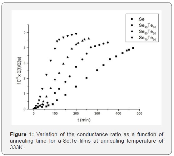
where σm is the conductivity of the partially crystallized layer during the annealing process and σa is the conductivity of theamorphous layer [10]. The crystallization velocity was obtained through the measurements of τ (time at which the linearity of Σ(t)/Σ(a) curve breaks off). The conductance variation during the isothermal annealing of amorphous films of Se:Te (Te = 0-30 at.% of Se) is shown in Figure 1. The crystallization time τ was obtained at each annealing temperature and corresponding growth rates vcwere calculated.

The crystallization process was seen to occur in three stages.
During the first stage (0

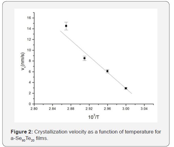
The crystallization velocity obtained in the experiment was found to decrease continuously with increasing Te concentration at each of the annealing temperatures. As is evident from Figure 2, the crystallization velocities show a thermally activation behaviour with an Arrhenian dependence for each of the composition given by [11]

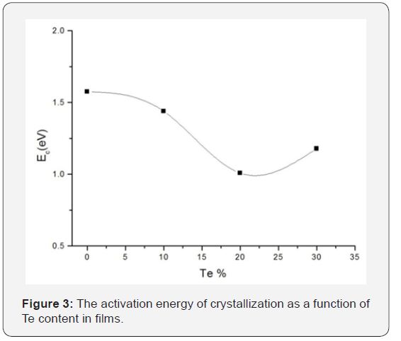
Figure 3 shows the dependence of the activation energy Ec of crystallization on the Te content. The pre-exponential of crystallization velocity also show same type of behavior. In the range x=0 to 20 at.% in Se: Te films, both Ec and vco decrease monotonically. The Te induced retardation was also observed in the melt quenched bulk glasses studied by us [6] and others [12]. With a further increase in Te, these quantities go through a minimum at 20 at.% Te. A similar compositional dependence of the activation energy of crystallization has been reported in melt quenched Se: Te bulk glasses by Ganaie et.al. [13].

The minimum in Ec can be understood as follows. The cis- (ring segment) and trans- (helical chain segment) configurationsin amorphous Se differ only in the placement of the 5th neighbor atom for molecular bondings [14]. The placement of the likely atom depends on the competition between the intra-chain and inter-chain forces. It is expected that the number of cisconfiguration starts to decrease near this configuration with increasing Te content, because the intra-chain force of Te is weaker than that of Se. The intra-chain force decreases and the inter-chain force increases with the addition of Te atoms to a-Se. The minimum activation energy at the particular Te concentration is therefore, likely to be attributed to such an intermediate range structural modification. The increase of glass transition temperature with Te concentration also indicates increasing chain lengths of Se-Te [15] and hence to a more rigid network.
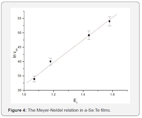
Figure 4 shows the plot of the pre-exponential factor vco versus the activation energy Ec of the crystallization velocity in thin films. There is a very good correlation between the vco and Ec, often referred to as the Meyer-Neldel relation [16] and is described as


Where vco is a constant with a value of about 1.8*10-3nm/s and Eco~0.0483eV as deduced from Fig.4. Here, the obtained value of Meyer-Neldel energy is 48.3meV, which is well within the range 25-100meV generally reported in semiconductors [17]. This energy corresponds to Meyer–Neldel temperature equal to 560K , that is within the reported range of temperatures 260-950K [ 18].
Assuming that the crystallization velocity in amorphous materials is inversely propotional to the viscosity of the melt η [12], which has a Vogel-Tammann-Fulcher type of behaviour [19], i.e., η=ηo exp (Eo / k (T-To)), where ηo, Eo and To are constants, then the crystallization velocity becomes

This equation is almost indistinguishable from Eqn. (2) in a narrow range of temperature except for the vicinity of To. Moreover, if we try to fit the Arrhenian dependence of vc in a temperature range T1 to T2 , we obtain [5]

Where

y1=a-b, y2= ln(a/b), y3=ln{(a - 1)/(b - 1)}, y4= (1/b)-(1/a), a= T2/To; b=T1/To.
The estimated Eco value of 0.0325eV is obtained using T1=330K, T2=360K and To=303K. This is an indication that the crystallization velocity in a-Se:Te films can be considered to be controlled by the viscosity of the melt. The variation in Vicker’s hardness in chalcogenides around crystallization temperatures also allows us to correlate our results with viscosity [20]. The increase in glass transition temperature with Te concentration is a good indicator of the increase in viscosity with Te [21].
Although the Meyer-Neldel relation has been observed in various physical systems, there is still no satisfactory uniform explanation for its occurrence. Several mechanisms to explain the origin of MNR in semiconductors have been proposed. Jakson [22] argued that whenever a multiple trapping transport process is observed as a function of temperature, MNR should be followed. Abtew et al. [23] have performed a comparative study of MNR in crystalline Si and non hydrogenated amorphous silicon and claimed that MNR is present in amorphous silicon only. They suggested that the existence of localized state and the energyelectron lattice coupling for these states is an essential feature of MNR in silicon amorphous phase. Thus, MNR presence is closely connected to the presence of band tail of localized states which are generally assigned to the disorder in film network.
In disordered semiconductors, three conduction mechanisms may occur:
- Hopping from one localized sates to another localized state.
- Carrier hopping from localized state to an available extended state.
- Carrier scattered from one extended state to am empty extended state.
The first two conduction mechanisms require phonon assistance. Transition (i) and (ii) plays a role at low and moderate temperature. However the transition (iii) may be significant only in higher temperature. The conductivity in the films is governed by the multi-trapping process in band tail localized states and explains the MNR observation in films.
The present system gives a wide band gap semiconductor with exponential localized tail states proposed by Roberts [24].Since the conduction mechanism in films involves localized states, the electronic transport is achieved through electrons trapping and detrapping by multi-phonon process with the contribution of many phonons. This conduction model was first suggested by Yelon and Movaghar to explain MNR in thermally activated conduction [25]. In localized states conduction, the activation energy of the transition from localized state with energy Ei to an empty localized state with energy Ej is given by [26].

Where Er is the reorganization energy of the semiconductor random network for carrier hopping and is expressed as

Where ϵi and ϵj are the localization radii for the two localized states, R is the distance between the two localization centers [27], e is the elementary electric charge, ϵ0 is the vacuum dielectric constant, ϵop and ϵs are optical and static dielectric constants respectively. With increasing the disorder, the distance R increases and the film density decreases, consequently the film refractive index and optical dielectric constant are reduced [28,29] This leads to the increase of the two square brackets in Eq. (8) and then to the increase in the reorganization energy Er and consequently the reduction of the activation energy Ea.
Conclusion
The conductance measurements carried out on SeTe glassy films between the glass transition and crystallization temperatures provides information about the crystallization mechanism in thin films. During the early times, the crystallization is due to nucleation and conductance varies quadratically with time. When the nucleation is completed, the conductance varies linearly and the process occurs as a result of growth of crystallites towards the surface. The addition of Te reduces the growth and activation energy show a minimum at x=0.6. Meyer Neldel relation is found to be obeyed in the present case through pre-exponential of velocity and activation energy. This can be assigned to an increase in localized states resulting in increase in viscosity of the specimen around Te 60 at%.
References
- Patial BS, Thakur N, Tripathi SK (2011) J Therm Anal Calorim 106: 845.
- Bhargava A, Kalla J, Suthar B (2010) Crystallization Process in Amorphous Sn-Te-Se Thin Films. Chalcogenide Letters 7(3): 175.
- Bhargava A, Kalla J (2016) International Journal of Materials Science and Engineering 4(2): 126-132.
- Yoon SM, Choi KJ, Lee NY, Lee SY, Park YS, et al. (2007) Nanoscale Observations on the Degradation Phenomena of Phase-Change Nonvolatile Memory Devices Using Ge2Sb2Te5. Japan J Appl Phys 46(2): 4-7.
- Nasu T, Naito H, Kurosawa K, Matsushita T, Okuda M (1989) Japan J Appl Phys 28(3): 285.
- Bhargava A, Williamson A, Vijay YK, Jain IP (1995) J Non-Cryst Solids 192 & 193: 494.
- Bhargava A (2017) An Interrelation between Electrical Conductivity, Cystallization Process and Meyer-Neldel Relation in a-SeTe Sn Films. International Journal of Materials Science 12(2): 321-328.
- Landauer R (1952) The Electrical Resistance of Binary Metallic Mixtures. J Appl Phys 23: 779.
- Germain P, Squelard S, Bourgoin JC, Gheorghiu A (1977) Crystallization in amorphous germanium J Non-Cryst Solids 23: 93.
- Bhargava A, Jain IP (1994) J Phys D Appl Phys 27: 830.
- Georgieva I, Nesheva D, Dimitrov D, Kozhukharov V (1993) J Non-cryst Solids 160: 105.
- Kasap SO, Juhasz C (1986) Kinematical transformations in amorphous selenium alloys used in xerography J Mater Sci 21(4): 1329-1340.
- Ganaie M, Ahmad S, Islam S, Zulfequar M (2004) Int J Phys and Astro 2(2): 51.
- Lucovsky G, Gallener FL (1980) J Non-Cryst Solids 35 & 36: 1209.
- Matsuishi K, Kasamara H, Onari S, Arai T (1989) J Non-Cryst Solids 114: 46 (1989).
- Meyer W, Neldel H (1937) Z Tech Phys 12: 307.
- Widenhorn R, Mundermann L, Rest A, Bodegom E (2001) Meyer– Neldel rule for dark current in charge-coupled devices. Journal of Applied Physics 89: 8179.
- Abdel Wahab F (2002) Journal of Applied Physics 91: 265.
- Elliott SR (1990) Physics of Amorphous Materials 2nd Edn. Longman, London.
- Kumar H, Sharma A, Mehta N (2014) Effect of Tin Incorporation on Thermo-Mechanical Properties of Glassy Se80Te20 Alloy. Chinese Phys Lett 31(3): 036201.
- Freitas RJ, Shimakawa K, Kugler S (2013) Chalcogenide Letters 39: 1091.
- Jakson WB (1988) Physical Review B38: 3595.
- Abtew T, Zhang M, Pan Y, Drabold DA (2008) Journal of Non Crystalline Solids 354: 2909.
- Roberts GG (1971) Thermally assisted tunnelling and pseudointrinsic conduction: two mechanisms to explain the Meyer-Neldel rule. J Phys C 4: 3167.
- Yelon Y, Movaghar B (1990) Physical Review Letters 65: 618.
- Reik HG (1972) In: Devereese JT (Edn.), Polarons in Ionic and Polar Semiconductors, Elsevier, North Holland.
- Marcus RA (1993) Review of Modern Physics 65: 599.
- Mahmoud SA, Ibrahim AA, Riad AS (2000) Thin Solid Films 372: 144.
- Mahdi, Kasem SJ, Hassen JJ, Swadi AA, Ani SKJA (2009) International Journal of Nanoelectronics and Materials 2: 16.


